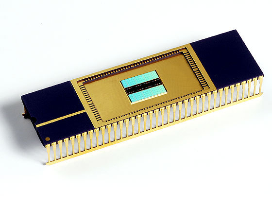
IBM: Phase Change Memory to Operate Beyond 150°C
IBM has been granted a patent for an exotic phase change memory (PCM) cell structure the allows the technology to retain its data retention characteristics at temperatures above 150 degrees Celsius (300 degrees Fahrenheit).
The patent, which was filed as an application in November 2009 and approved on July 31, 2012, describes a memory cell that uses techniques such as insulation material as well as growth-dominated phase change material to achieve "superior" memory qualities at increasing temperatures. The inventors explain that a current sent through the phase change material creates ohmic heating and causes the phase change material to melt.
Phase change memory is based on the idea of taking advantage of behavior of chalcogenide glass, which can assume crystalline and amorphous states, depending on the temperature. Gradual cooling results in a crystalline state of the material and abrupt cooling quenches the phase change material into the amorphous state. Once quenched, the crystallization temperature decreases "and the amorphous region is surrounded by a crystalline layer which acts as a seed for growth," the patent states. The problem: "If the phase change memory cell is raised to a higher temperature, the data stored within the memory cell may be lost or degraded due to changes in the size and shape of the amorphous region."
IBM's solution is a phase change memory cell with the characteristics of
- A bottom electrode
- A top electrode separated from the bottom electrode
- Growth-dominated phase change material deposited between the bottom electrode and the top electrode and contacting the bottom electrode and the top electrode and surrounded by insulation material at sidewalls thereof
- The phase change memory cell in a reset state only includes an amorphous phase of the growth-dominated phase change material within an active volume of the phase change memory cell
- The phase change memory cell comprises a current path that includes interface regions between the bottom electrode
- The growth-dominated phase change material and the top electrode such that a reset current at a predetermined value above the nominal reset condition flows along the current path
- The growth-dominated phase change material is fully amorphized after the reset operation, and wherein the interface regions comprise gallium (Ga) atoms
There is no information of a commercial application of the patent.
Contact Us for News Tips, Corrections and Feedback
Get Tom's Hardware's best news and in-depth reviews, straight to your inbox.

Douglas Perry was a freelance writer for Tom's Hardware covering semiconductors, storage technology, quantum computing, and processor power delivery. He has authored several books and is currently an editor for The Oregonian/OregonLive.
-
aoneone so what happens beyond this memory idea, is that increasing temperatures will forever hold any data information forever, thus making it practically indestructible.Reply
In other words, porn viewers downloading data and info onto their harddrives and thinking you can wipe it away by burning it .. ha fat chance pervert!! -
sylvez aoneoneso what happens beyond this memory idea, is that increasing temperatures will forever hold any data information forever, thus making it practically indestructible. In other words, porn viewers downloading data and info onto their harddrives and thinking you can wipe it away by burning it .. ha fat chance pervert!!Reply
... why pervert?? Internet is for porn.
Back to topic, IBM really needs to file another patent of this with rounded corners just in case.
-
falchard This patent is way to generic. Are you kidding me? A specific material setup in a specific way for a specific purpose with a working model. Better luck next time IBM on your broad implementation of a specific method of memory cooling. I think we all came up with this common method for use a special glass material.Reply -
K2N hater sylvezBack to topic, IBM really needs to file another patent of this with rounded corners just in case.Phase chips have a cold side and a hot side. Guess some IBM engineer switched the side, melted the whole thing and now patented the mess.Reply -
razor512 I wonder, what is the endurance of the various phase change chips coming out?Reply
there are a few in development but since it is relying on what pretty much a chemical reaction or a gas meaning you are dealing with relatively short half lives (reason why plasma screens don't last as long), and other forms of decay.
if it is just designed for NV storage, then it can be good for machines that work in hot environments, or at least bring technology one step closer to designing a rover that can function on a planet such as Venus. -
shin0bi272 So not only is it 100x faster than flash and lasts for millions of write cycles and is cheaper to produce than flash but now it even operates in temperatures well above what flash can do... Sooo why do we not have this in a hard drive yet there IBM? Whats the hold up?Reply
