Intel Charts Course to Trillion-Transistor Chips: 2D Transistor Materials, 3D Packaging Research
Intel's IEDM 2022 research papers hold promising new tech.
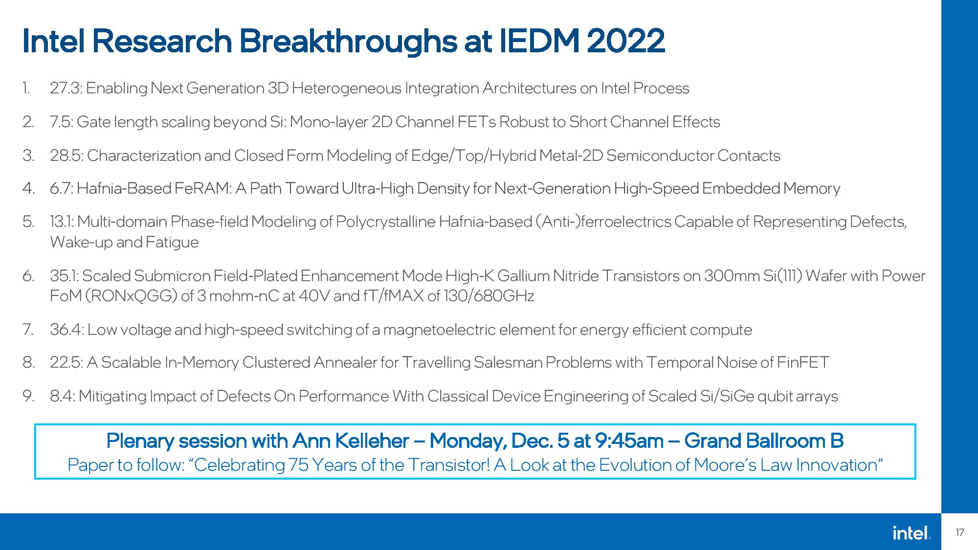
Intel released nine research papers at IEDM 2022 that lay the groundwork for future chip designs as the company looks to deliver on its promise of developing processors with over a trillion transistors by 2030.
The research includes new 2D materials for transistors, new 3D packaging technology that narrows the performance and power gap between chiplet and single-die processors to a nearly-imperceptible range, transistors that 'don't forget' when power is removed, and embedded memories that can be stacked directly on top of transistors and store more than one bit per cell, among other innovations.
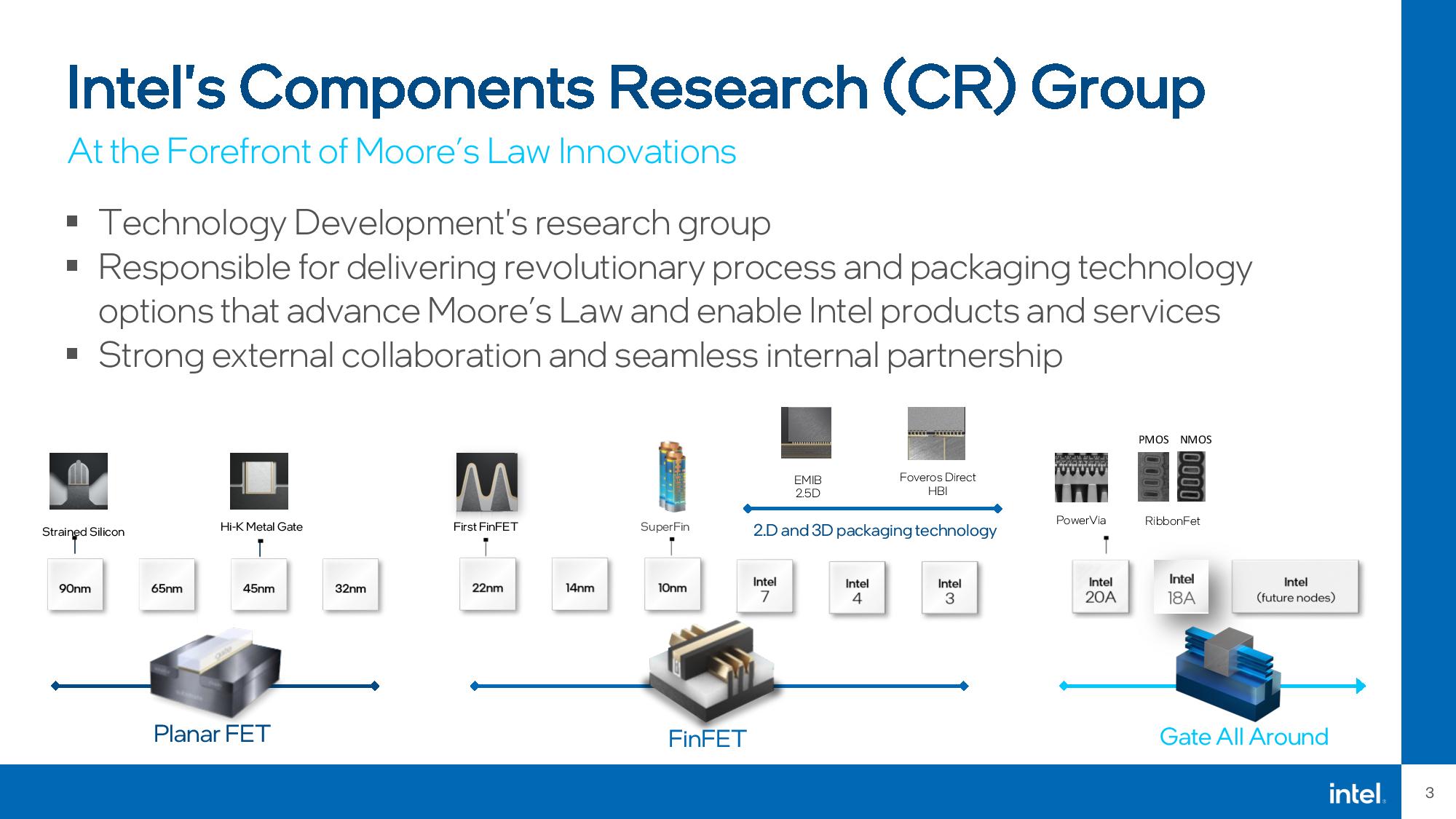
Intel's Components Research (CR) Group lays the initial groundwork for the company's future technologies, but not all of these initiatives will result in products that ship to market. Those that do come to market would typically arrive in five to ten years.
The group has an incredible track record of innovations that have already come to market, like FinFET, which revolutionized transistor design for the entire industry, strained silicon, Hi-K metal gate, and many others. Intel already has several other technologies on its roadmap, including RibbonFET Gate All Around (GAA) transistors, PowerVia back-side power delivery, EMIB, and Foveros Direct, which all hail from this research group.
The group submitted nine research papers at this year's 68th-Annual IEEE International Electron Devices Meeting, and below, we'll cover a few of them in slightly more detail. However, Intel hasn't yet presented the papers at the conference, so this is broad coverage of the topics.
The pace of transistor density increases continues roughly in line with Moore's Law, but the economics of today's chips are not improving at the same pace — the price per transistor is rising as we move to denser nodes. In addition, poor scaling of some chip elements, like analog and caches, complicates matters further. As such, the industry is moving en masse to chiplet-based designs for high-performance chips.
The overriding goal of any chiplet-based design is to preserve the best attributes of the power consumption and performance (latency, bandwidth) of the data pathways inside of a single-die monolithic processor while tapping the economic benefits of using a chiplet-based approach, like increased yield from smaller dies fabbed on a leading-edge process and the ability to use older, cheaper nodes for some of the other functions that see lesser density improvements.
As such, the battleground for semiconductor supremacy is shifting from the speed of the transistors to the performance of the interconnects, with new technologies like silicon interposers (EMIB) and hybrid bonding techniques coming to the forefront to improve economics.
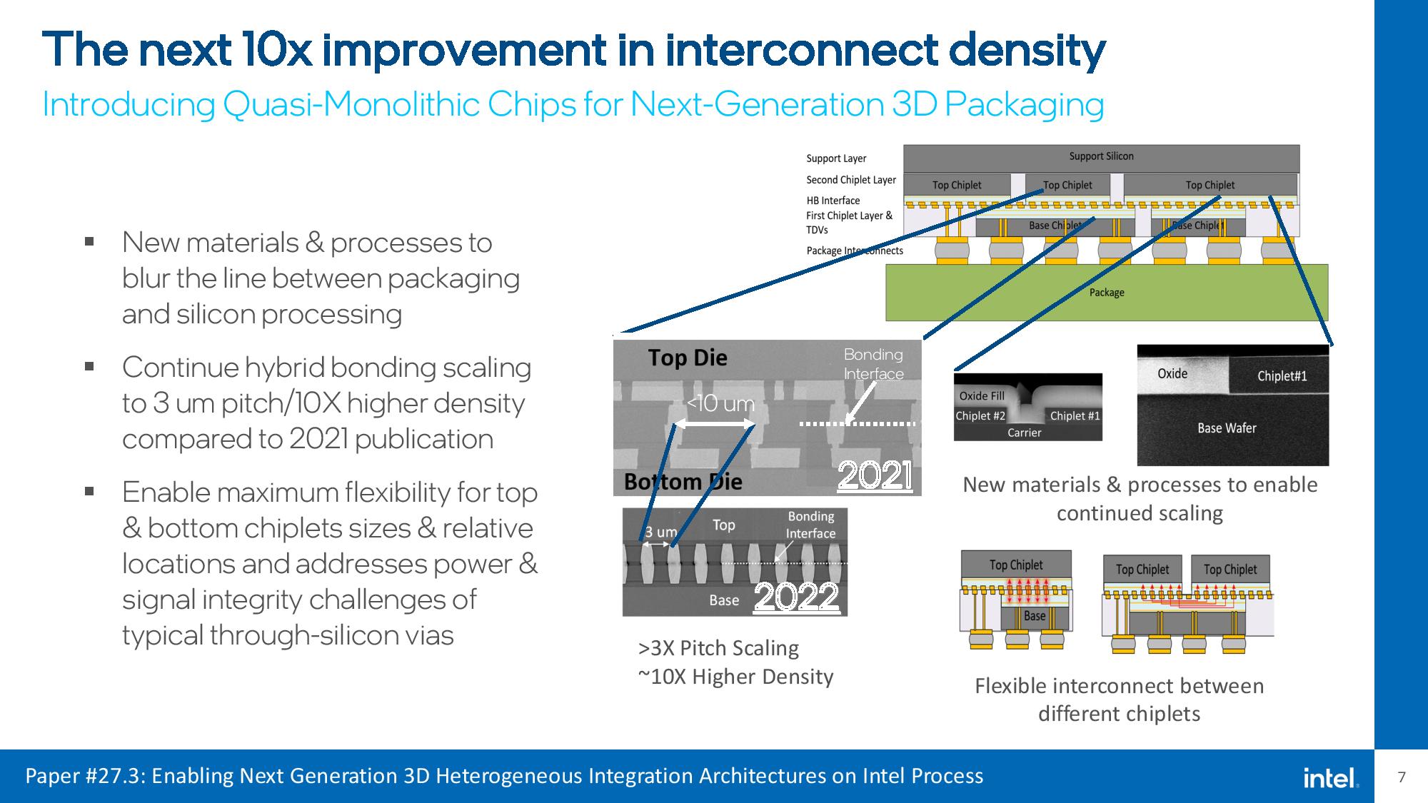
However, these approaches still result in inevitable performance, power, and cost tradeoffs, which Intel's new 'Quasi-Monolithic Chips' (QMC) 3D packaging tech looks to solve. As the name implies, Intel's QMC aims to offer nearly the same characteristics as the interconnects that are built right into a single die.
QMC is a new hybrid bonding technique that features sub-3 micron pitches and results in a 10X increase in power efficiency and performance density over the research Intel submitted at last year's IEDM. That previous paper covered an approach with 10-micron pitches, which was already a 10X improvement. As such, Intel has found a pathway to a 100X improvement in just a few years, showing that the company's work in hybrid bonding is accelerating rapidly. QMC also enables multiple chiplets to be stacked vertically atop one another, as seen in the graphic above.
This paper outlines incredible interconnect densities of hundreds of thousands of connections per square millimeter and power consumption (measured in picojoules per bit - Pj/b) that rivals what we see in monolithic processors. In addition, the new paper outlines several new materials and processes that would be used to manufacture such devices, paving the way for real-world devices.
Get Tom's Hardware's best news and in-depth reviews, straight to your inbox.
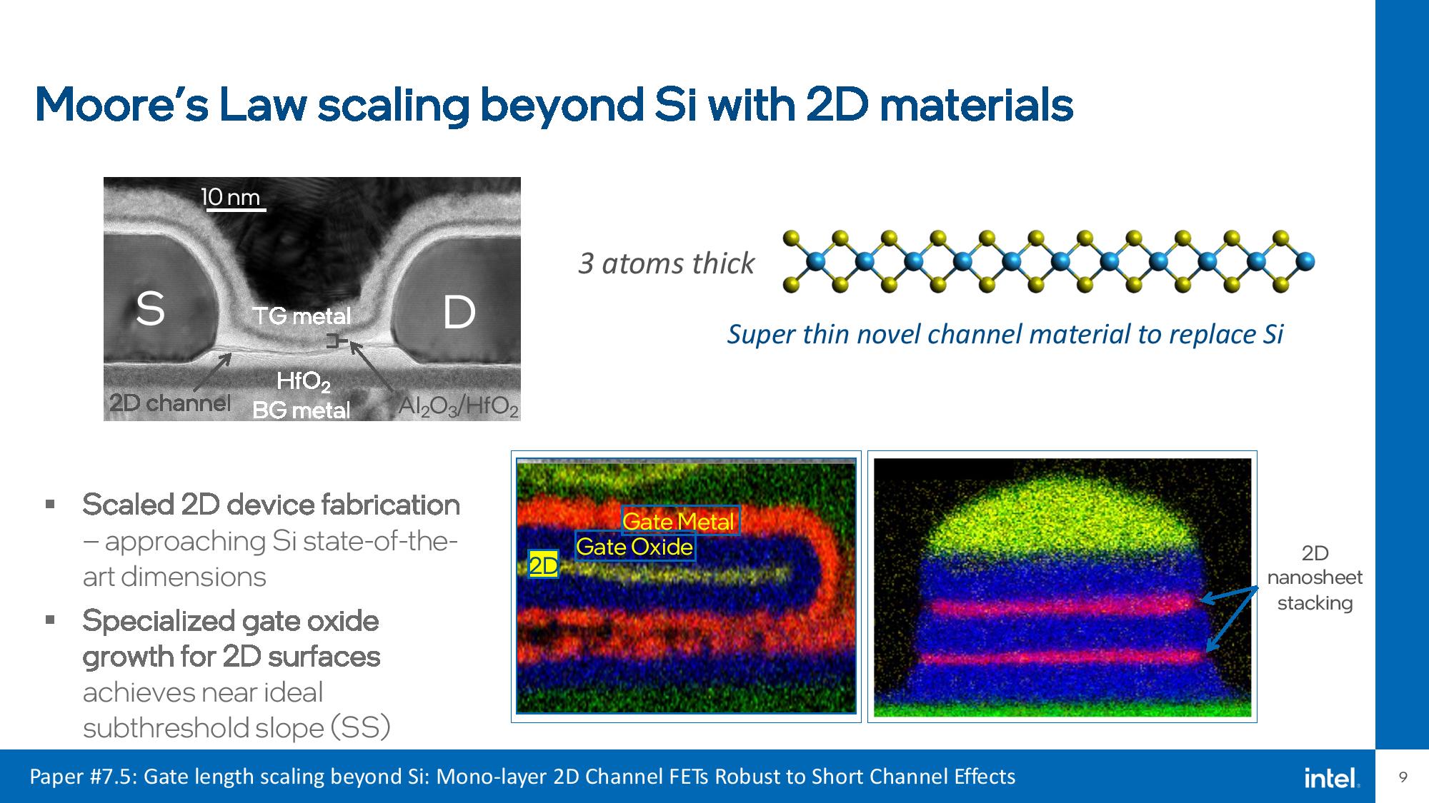
Intel's process roadmap already dips below the nanometer scale to the Angstrom scale, and even though the node naming conventions have long ago lost their relation to actual physical measurements of the transistors, it is clear that a radical new approach will be needed for continued scaling. Most of the industry is betting on a shift to 2D atomic channels in the future, but as with all new tech, there will be many steps to such a radical change.
Today's chip materials, like silicon, are comprised of three-dimensional crystals, which means atoms are bonded in all three dimensions, thus presenting a fundamental limit to shrinking. In contrast, 2D materials are attractive because all of the atoms are bonded in one plane, thus enabling features to be built with as small as three atoms of thickness.
Enter Intel's research into 2D materials that it could use for 3D GAA transistors. As a refresher, current GAA designs consist of stacked horizontal silicon nanosheets, with each nanosheet surrounded entirely by a gate. This 'gate-all-around' (GAA) technique reduces voltage leakage that prevents switching off the transistors. This is becoming more of an issue as transistors shrink — even when the gate surrounds the channel on three sides, as we see with FinFET transistors.
Intel brands its GAA design as RibbonFET, which is currently planned to arrive in the first half of 2024. However, moving beyond RibbonFET will require further innovations, and this 2D research fits the bill of a potential pathway.
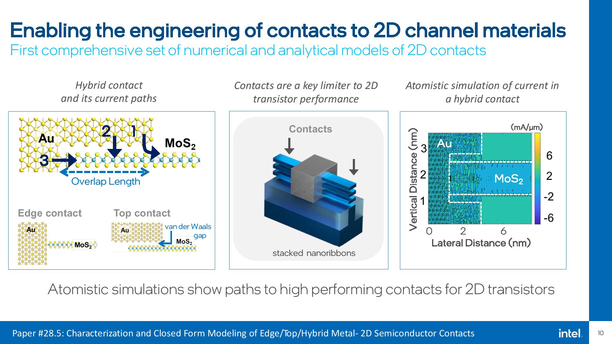
Intel's paper describes a Gate All Around (GAA) stacked nanosheet structure with channel materials (nanosheets/nanoribbons) that measure a mere three atoms thick and can operate at room temperature with low leakage current.
The thinness of 2D channel materials makes establishing an electrical connection to a nanoribbon a daunting task, so Intel also modeled electrical contact topologies for 2D materials. This is a key step to understanding the properties of the 2D materials and how they function, thus allowing the company to accurately model further advancements.
Memory in all forms is an integral part of computing, but it also consumes plenty of the power budget at both the chip and system level while also being a limiting factor for performance.
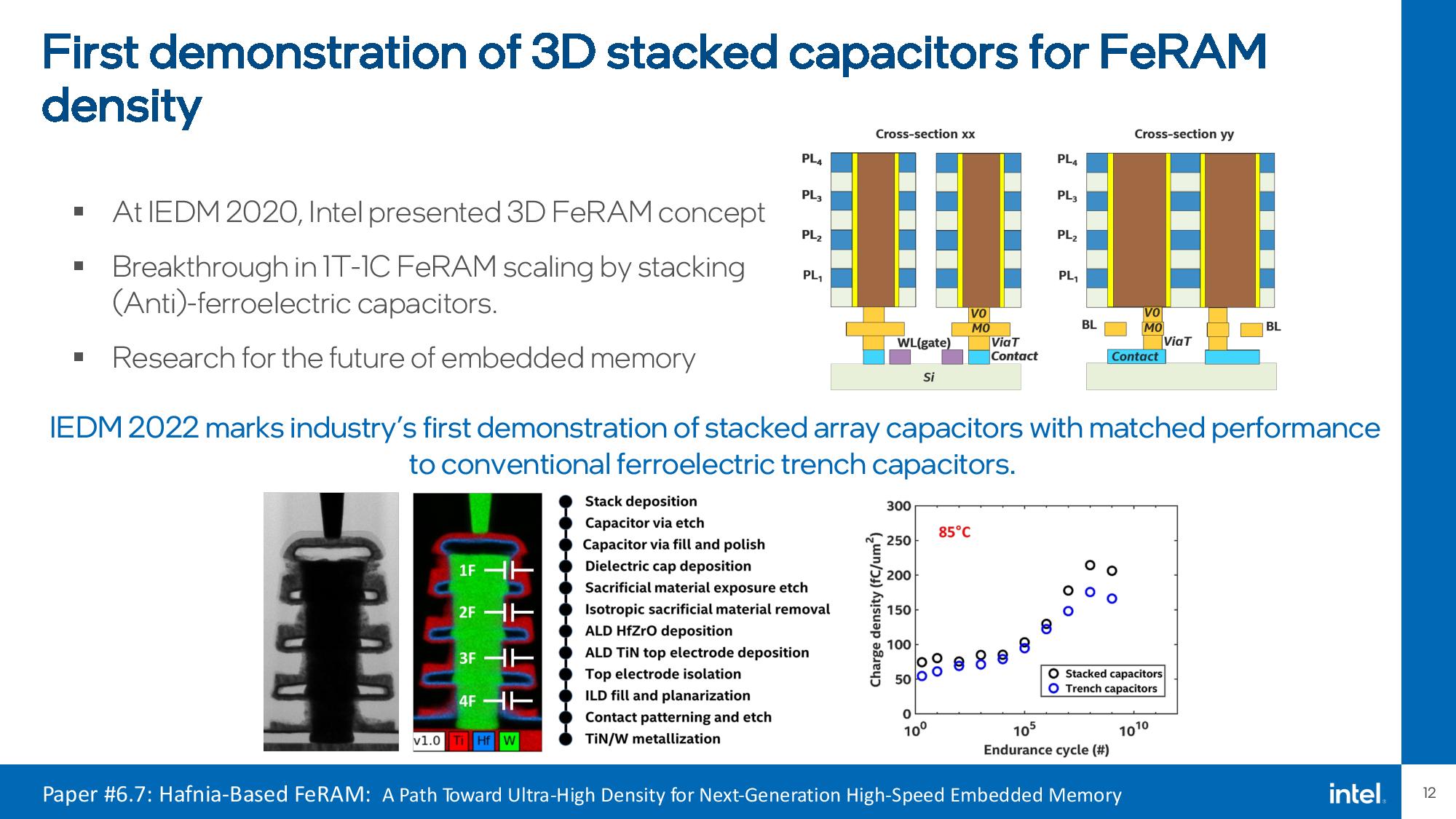
Intel also conducted the world's first functional demonstration of 3D-stacked ferroelectric memory. The most impressive aspect of this tech is that ferroelectric trench capacitors can be stacked vertically on the logic die atop the transistors. That enables layering the memory atop the logic elements instead of being in its own distinct region, as we see with other types of embedded memory, like SRAM used for L1 and L2 caches.
Ferroelectric memory also enables a similar capability to what we see with NAND flash — the ability to store multiple bits of data in a structure that would typically only store one bit. In this case, Intel demonstrated the ability to store four bits per trench.
Naturally, this approach would increase both bandwidth and memory density while reducing latency, yielding much larger and much faster on-chip caches.
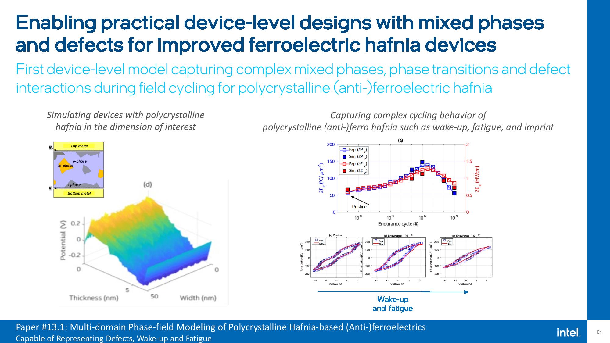
In the same vein as the electrical contacts modeling for 2D structures, Intel also shared its modeling efforts for mixed phases and defects for ferroelectric hafnia devices, which will, in turn, further the company's own research and development processes.
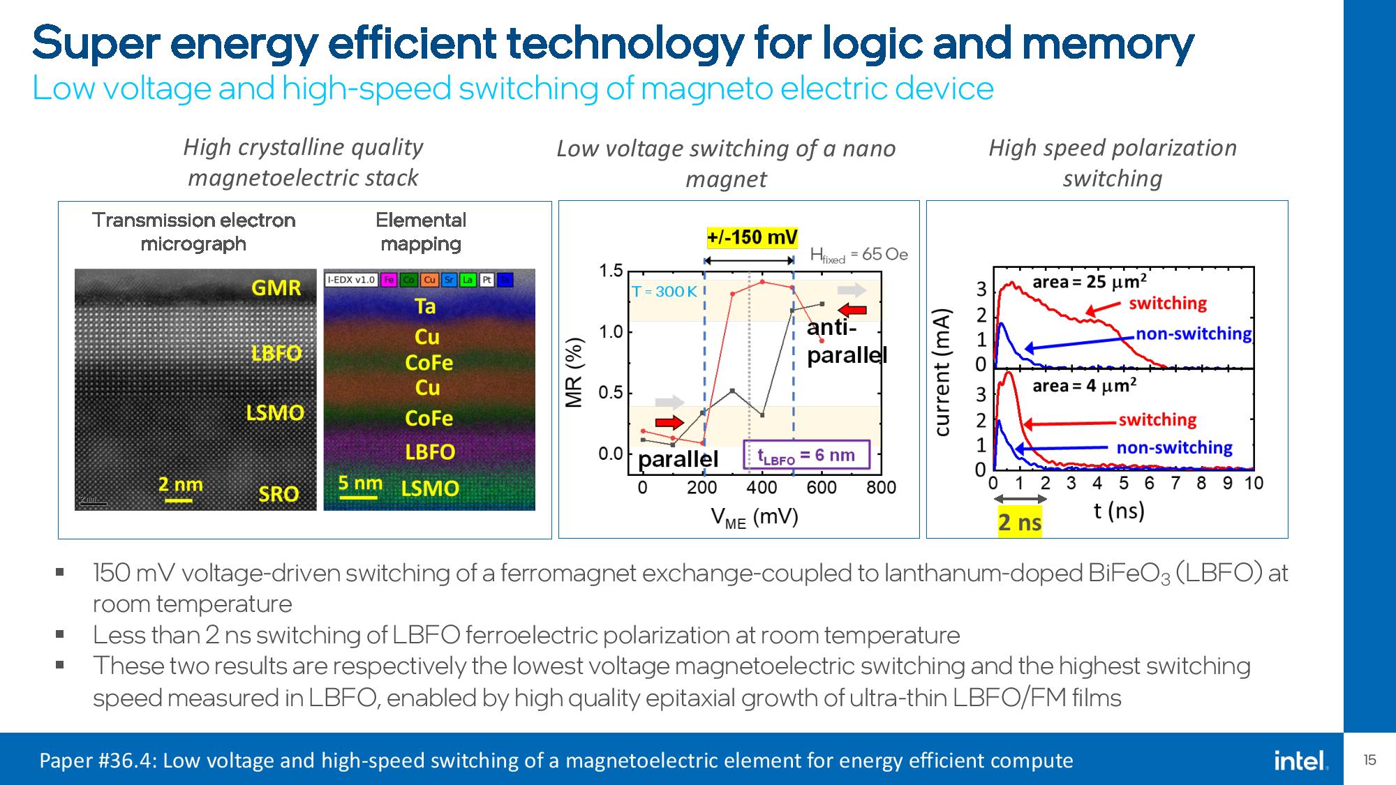
Intel is also researching transistors that 'don't forget,' meaning they don't lose their data (on/off state) when they lose power. This is akin to any non-volatile storage, like NAND, that can retain its state when power is removed, but it comes in the form of a logic transistor. Intel says it has hurdled two of the three roadblocks to using this technology at room temperature. We're particularly looking forward to this presentation.
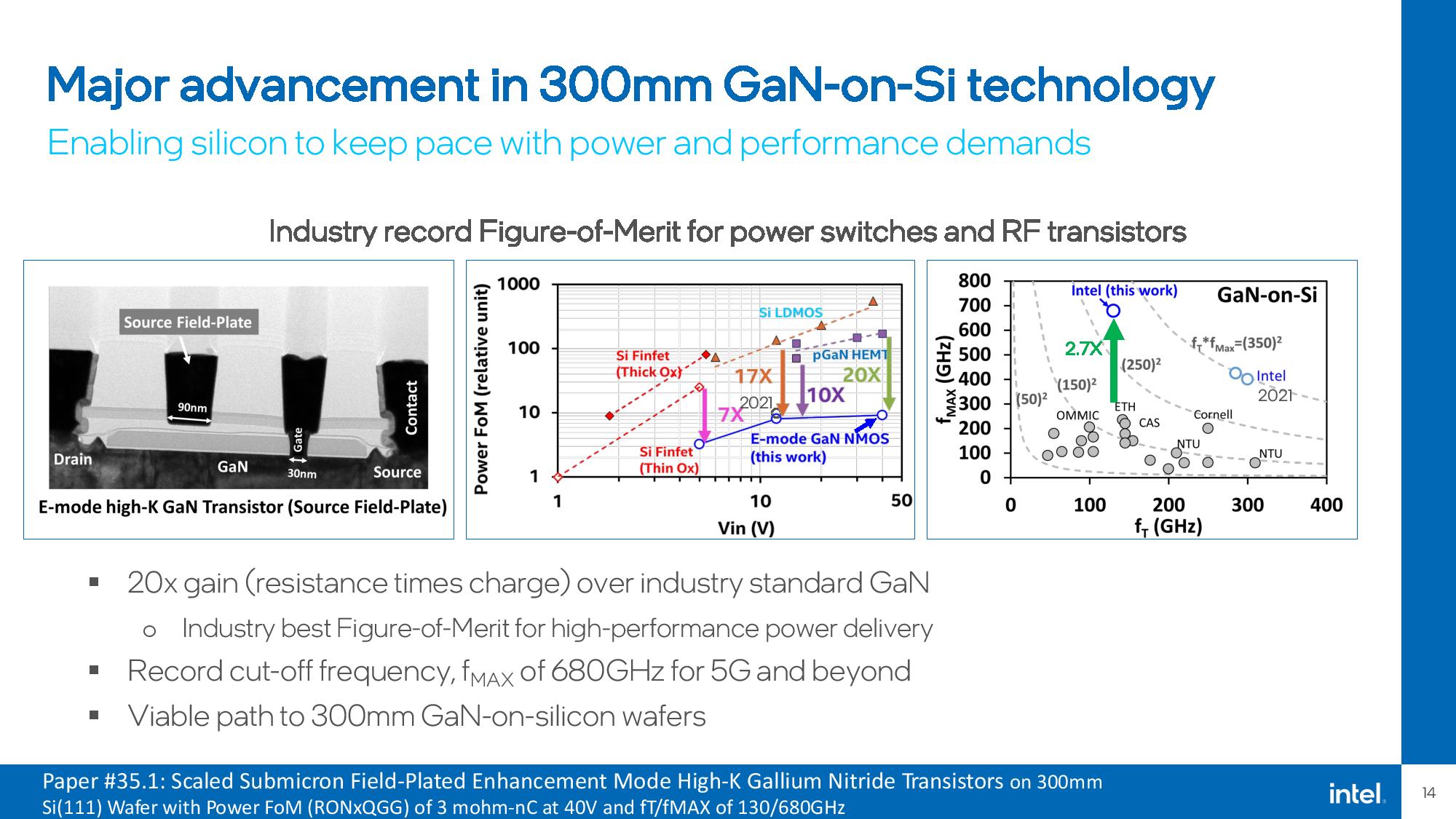
Intel's other papers at the event outline other research areas, like GaN-on-silicon wafers that can enable future technologies beyond 5G, and better ways to store quantum information to create better qubits for quantum computing.
It's been 75 years since the transistor altered the course of history, and Intel's Dr. Ann Kelleher, the VP and GM of Technology Development, will also give a special address at IEDM on Monday. The "Celebrating 75 Years of the Transistor! A Look at the Evolution of Moore’s Law Innovation" presentation takes place at 9:45 am PT on Monday, December 5. We'll follow up with coverage of that presentation soon.

Paul Alcorn is the Editor-in-Chief for Tom's Hardware US. He also writes news and reviews on CPUs, storage, and enterprise hardware.
-
Geef Hearing things like this is great but I'm hoping there are places with actual printed paper data of how to do all this. I'd hate for an EMP blast to happen and wipe the entire planet out and we lose XX years of top tech like this.Reply -
TechieTwo ReplyGeef said:Hearing things like this is great but I'm hoping there are places with actual printed paper data of how to do all this. I'd hate for an EMP blast to happen and wipe the entire planet out and we lose XX years of top tech like this.
The paperless office ended 40 years ago... or at least it was suppose too. -
Reply
The kind of EMP blast you’re talking about would bring about way worse problems than thisGeef said:Hearing things like this is great but I'm hoping there are places with actual printed paper data of how to do all this. I'd hate for an EMP blast to happen and wipe the entire planet out and we lose XX years of top tech like this.
in other words, it would be cataclysmic, and you would have other things to worry about than this nonsense. like basic survival -
digitalgriffin Reply
No place on earth would be safe even in a limited war. Even if you could disregard nuclear winter, and ground + water contaminated with cesium and strontium, you would have to deal with likely dozens of nuclear power plants that likely melted down and had core failures because all methods of cooling them would also be destroyed. The cooling services are external to the containment building. Imagine Chernobyl except no emergency services left because infrastructure has been destroyed and entire area is a hot zone.Mandark said:The kind of EMP blast you’re talking about would bring about way worse problems than this
in other words, it would be cataclysmic, and you would have other things to worry about than this nonsense. like basic survival
It's not MAD. It's everyone and every creature suffers destruction. -
russell_john A pretty bold claim for a company that has struggled for years just to make 7nm work for them ......Reply -
digitalgriffin Replyrussell_john said:A pretty bold claim for a company that has struggled for years just to make 7nm work for them ......
It's like a jigsaw puzzle. You find all the edge pieces , put them in place then slowly fill them in. You have to start somewhere. -
TerryLaze Reply
The only thing intel struggled with was making 14nm stop being profitable...russell_john said:A pretty bold claim for a company that has struggled for years just to make 7nm work for them ......
They made so much money off the old tech that it would be crazy to come out with something new.
Intel 7 isn't 7nm, it's 10nm, and even that they halve down and supplement with crappy small cpus and they still make all of the money. -
Wisecracker Pretty much this.Reply
See: IEDM 2018: Intel’s 10nm Standard Cell Library and Power Delivery3 Main Library Offerings
Through considerable analysis, Intel arrived at three main logic library offerings – a high-density cell, a high-performance cell, and an ultra-high performance cell. All three libraries are 6T libraries, each with a custom-designed BEOL.
Short Library – HD Cells – cells can accommodate 2 fins per cell height, 2p+n
Mid-Height Library – HP Cells – cells can accommodate 3 fins per cell height, 3p+n
Tall Library – UHP Cells – cells can accommodate 4 fins per cell height, 4p+nrussell_john said:A pretty bold claim for a company that has struggled for years just to make 7nm work for them ...... -
Endymio ReplyThis paper outlines incredible interconnect densities of hundreds of thousands of connections per square millimeter and power consumption (measured in picojoules per bit - Pj/b)
Pj/b is a measure of energy consumption per bit, not power.
Nuclear winter is an entirely discredited theory.digitalgriffin said:No place on earth would be safe even in a limited war. Even if you could disregard nuclear winter...
...you would have to deal with likely dozens of nuclear power plants that likely melted down....
And? All modern plants have multiple power backup facilities. Even if those were taken out (which a limited war would NOT do) the plants also have concrete containment sarcophagi. The results would be not like Chernobyl, but like Japan's Fukushima, an accident that caused zero deaths from acute radiation sickness. There were a total of 160 workers at Fukushima would receivedwhole-body doses of around 100 mSv, or around what the average person already receives every 15 years just from natural background sources.