Intel Has 5 nm Processors in Sight
Every once in a while, Intel restores our confidence that Moore's Law is still alive and well.
Get Tom's Hardware's best news and in-depth reviews, straight to your inbox.
You are now subscribed
Your newsletter sign-up was successful
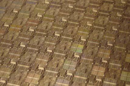
According to the company, future production processes down to 5 nm are on the horizon and will most likely be reached without significant problems. Following the current 22 nm process, Intel's manufacturing cadence suggests that the first 14 nm products will arrive in late 2013, 10 nm in 2015, 7 nm in 2017, and 5 nm in 2019. A slight adjustment has been made to include different production processes for traditional processors and now SoCs. The company previously indicated that SoCs will be accelerated to catch up with the process applied to Intel's main processor products.
According to reports, Intel does not see any reason to believe that Moore's Law, which is really more an accepted guideline and observation rather an actual "law", will be breached by the company within 10 years, which indicates that Intel has visibility even beyond 5 nm. At this time, Intel has 14 nm in development, and 10 nm manufacturing in its research phase.
Also, Intel said that it is planning to move from 300 mm to 450 mm production wafers, but this switch is still about five years out. There was no information on the introduction of EUV lithography.
Article continues belowContact Us for News Tips, Corrections and Feedback
Get Tom's Hardware's best news and in-depth reviews, straight to your inbox.

Wolfgang Gruener is an experienced professional in digital strategy and content, specializing in web strategy, content architecture, user experience, and applying AI in content operations within the insurtech industry. His previous roles include Director, Digital Strategy and Content Experience at American Eagle, Managing Editor at TG Daily, and contributing to publications like Tom's Guide and Tom's Hardware.
-
DRosencraft Should be very interesting to see how this turns out. That will be some impressive tech. Better start saving now and hope they're right about not hitting any roadblocks, although they probably have no real functional idea otherwise they'd just make the effort to go straight there. Nothing wrong with the step-by-step approach though. Wish them luck in overcoming Moore's Law.Reply -
edogawa 14nm processors in late 2013? Sweet, that's about the time I will upgrade from Sandy-Bridge.Reply
Glad to see Intel is moving forward without issues. -
balister Unfortuneately, Intel is about the hit the wall in how far they can go. 1 nm is pretty much the wall as that's about 5 atoms in width. Quantum effects start to take over once you get to that level and it is not as easily dealt with due to things like Heisenberg's Uncertainty Principle and how the Strong and Weak forces start being a much bigger factor.Reply -
ben850 LOL I'm still rocking a Phenom II x6 on my AM2+ setup.. Looks like my next upgrade could be an extremely huge leap in CPU technology :)Reply -
sebooker Just wondering....what kind of cooling is needed for a processor of those single-digit sizes?Reply -
buzznut balisterUnfortuneately, Intel is about the hit the wall in how far they can go. 1 nm is pretty much the wall as that's about 5 atoms in width. Quantum effects start to take over once you get to that level and it is not as easily dealt with due to things like Heisenberg's Uncertainty Principle and how the Strong and Weak forces start being a much bigger factor.Agreed, quantum computing is where I'd be investing my R&D right now. I think they will have problems before 2019.Reply -
blazorthon Six to eight years from now is not really "in sight" in this industry. Anything and everything can change in less than half of that time as far as this information is concerned. Saying that this will happen by 2019 doesn't mean that it won't be delayed until around 2025 or something like that. I'm also not convinced that 14nm will even hit the market for Intel until 2014 given that it would mean that Intel has about a year to get both Haswell and the 14nm die shrink of it (Broadwell if I remember correctly) and the chances of Haswell having a full line-up by the end of 2013 aren't even looking very good given that Ivy only got CPUs from all families Celeron and up a few days ago.Reply -
TeraMedia @balister:Reply
The problem is worse than that. If you consider that the typical doping level for an n-channel or a p-channel is on the order of 1:1000 atoms, then that means you need to actually have 1000 atoms for one of them to be doped (replacing Si with some other atom in the lattice). So a structure that is only 25 atoms wide by 25 atoms long is only 625 atoms per atomic layer. I remember reading somewhere that they need a minimum number of doped atoms for there to be any actual electrical effect, but I don't remember what that number was. -
jkflipflop98 balisterUnfortuneately, Intel is about the hit the wall in how far they can go. 1 nm is pretty much the wall as that's about 5 atoms in width. Quantum effects start to take over once you get to that level and it is not as easily dealt with due to things like Heisenberg's Uncertainty Principle and how the Strong and Weak forces start being a much bigger factor.Reply
Well good thing YOU were here to point that out!!! I'm sure none of the engineers and scientists at Intel have been poring over this exact problem for the last 10 years or so. Jesus P. Christ on a water buffalo I better got those dudes on the horn and share your revelation!
