Intel Lists Ponte Vecchio XT: A Higher-End Variant?
Raja sticks to his AMD roots with XT nomenclature

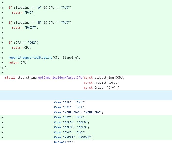
Intel's latest C for Metal compiler adds support for the company's current and upcoming integrated and discrete GPUs, including the codenamed DG2 family of gaming GPUs, aka Intel Arc Alchemist, as well as the future Ponte Vecchio compute GPUs. Based on the code, the Ponte Vecchio compute line-up will have at least two SKUs, including "Ponte Vecchio XT."
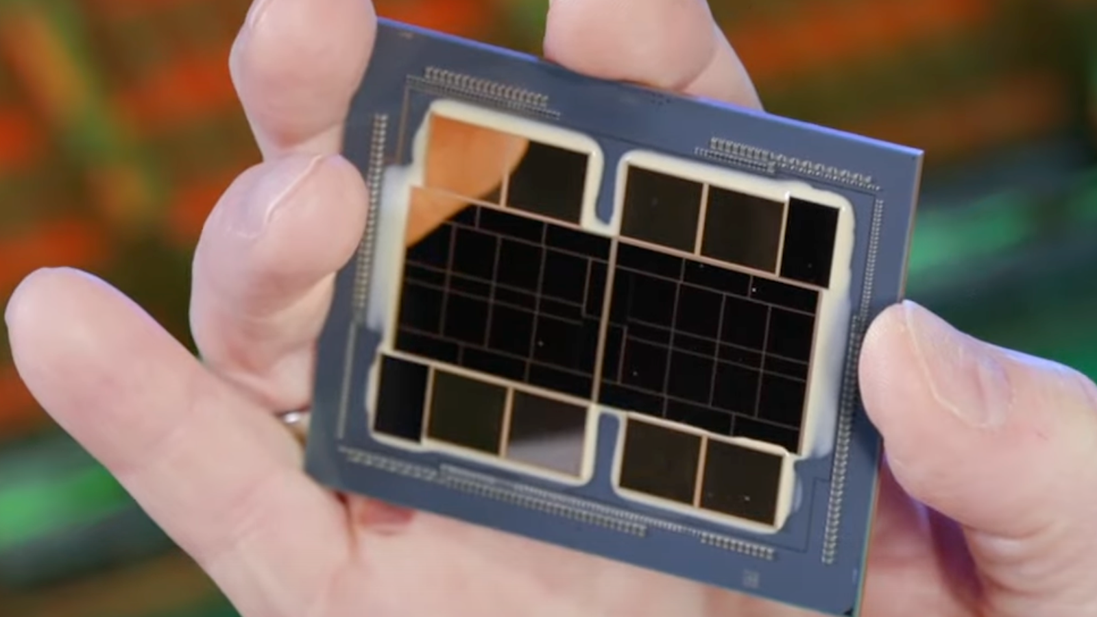
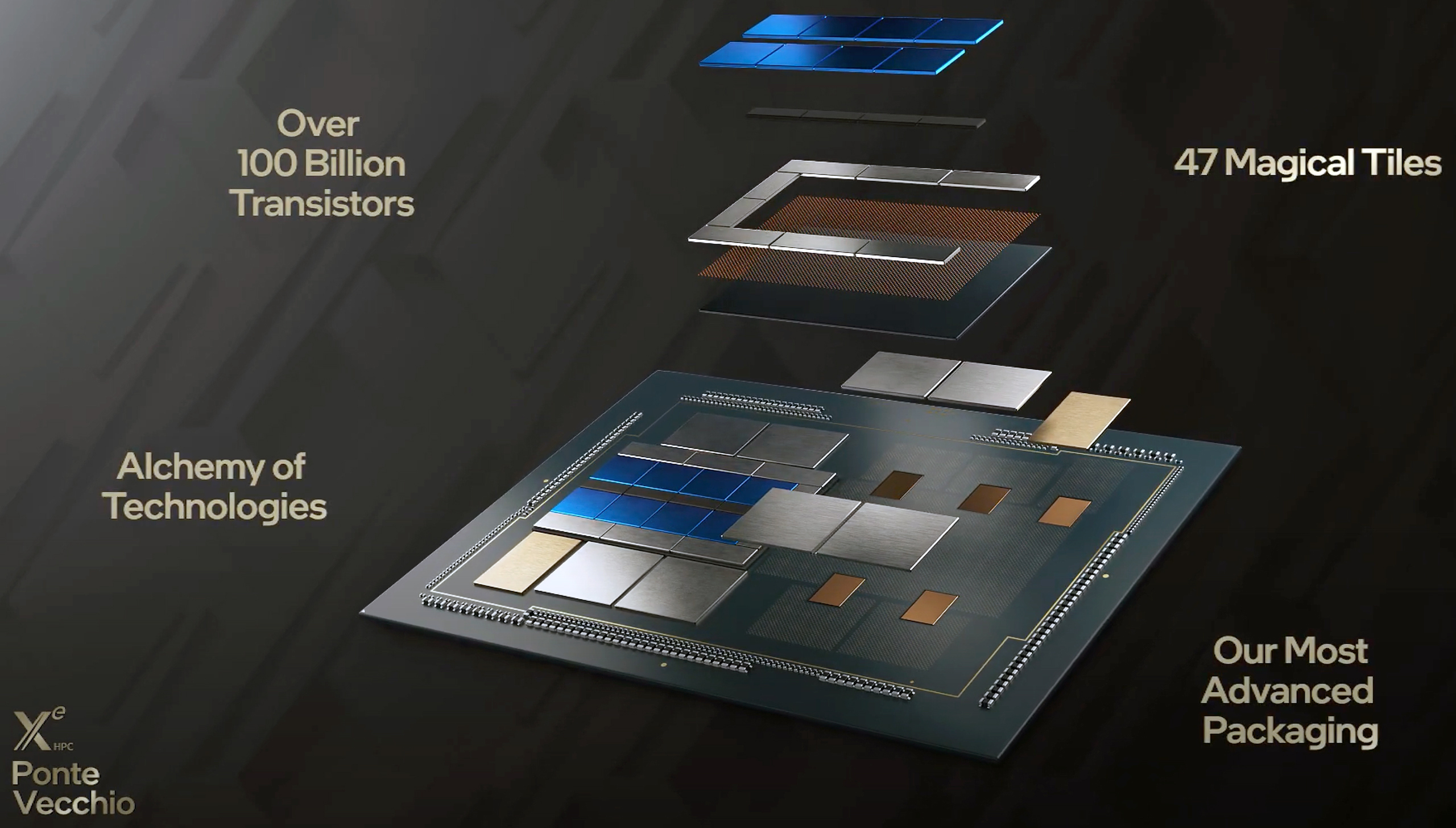
Intel's Ponte Vecchio is the company's flagship compute GPU that contains 100 billion transistors and is set to power the 2 ExaFLOPS Aurora supercomputer. The part features 47 components that will be made at different fabs using a variety of process technologies. But as discovered by Phoronix, there will be two versions of this GPU: the Stepping A called Ponte Vecchio (PVC) and the Stepping B called Ponte Vecchio XT (PVCXT). There might be additional variants in the future.
Ponte Vecchio includes the following tiles/chiplets:
- 2 base tiles made using Intel's 10 nm SuperFin technology
- 16 compute tiles produced by TSMC initially and then by Intel when its 7nm technology is ready for high-volume manufacturing (HVM).
- 8 Rambo cache tiles fabbed using Intel's 10 nm Enhanced SuperFin process
- 11 EMIB links made by Intel
- 2 Xe Link I/O tiles made by a foundry
- 8 HBM memory stacks produced by a DRAM manufacturer
Chip designers tend to not make many revisions of their flagship products as it can be expensive and chip production volumes are relatively limited. Furthermore, top-of-the-range compute accelerators are in many cases offered in just one configuration. This is true for AMD's Instinct MI250 and Nvidia's A100, though the core GPUs can then be configured with lower spec variants (often using harvest chips that otherwise can't hit the higher target designs). Ponte Vecchio may be taking a slightly different approach.
Intel has traditionally offered its compute accelerators (i.e., Xeon Phi) in several configurations, so offering regular Ponte Vecchio and extended Ponte Vecchio XT would be consistent with Intel's previous approach. After all, Ponte Vecchio will have to address numerous applications, including supercomputers, less powerful high-performance computing (HPC) deployments, and datacenters, so Intel will have to differentiate its offerings somehow.
There is another possibility as well. Back in 2020, Intel said that it would use TSMC's N5 process technology to produce the compute tiles of Ponte Vecchio in a bid to meet the schedules for the Aurora supercomputer, but then it would produce the same tiles using its own 7nm node (now called Intel 4) for later versions of PVC. While in 2021 the company ceased to talk about using its own fab to make the compute tiles, it does not necessarily mean that the plan has been abandoned. Furthermore, calling the initial version of PVC Stepping A and subsequent version with an in-house made compute tile as Stepping B makes sense.
One interesting thing to note is that the XT moniker used to describe the PVC Stepping B has been ATI's and then AMD's way to refer the top performing versions of its GPUs with more stream processors and/or higher clocks. Raja Koduri, Intel's GPU chief, previously worked at ATI and AMD for over 10 years, so it looks like those old habits of using the XT moniker have migrated to Intel.
Now, if the XT moniker of the Ponte Vecchio Stepping B indeed means extended, it begs the question how exactly the part is extended compared to the Stepping A. Will it have more cores, higher clocks, lower power characteristics, or perhaps all of the above? We'll learn more in the coming months.
Get Tom's Hardware's best news and in-depth reviews, straight to your inbox.

Anton Shilov is a contributing writer at Tom’s Hardware. Over the past couple of decades, he has covered everything from CPUs and GPUs to supercomputers and from modern process technologies and latest fab tools to high-tech industry trends.

