Intel: 14th Gen Meteor Lake Compute Tile Powers On, Performs Well
Meets all expectations.

Intel this week said that it successfully powered on a compute tile of its next-generation Meteor Lake processor that is expected to hit the market sometime in 2023. The compute tile is the company's first fairly complex chip made using its Intel 4 (I4) fabrication process, which indicates that the node is rather healthy two years before its commercial deployment. Intel said that the chip demonstrated performance in line with its expectations for this phase of the CPU development cycle.
"On Intel 4, we had taped out our compute tile for Meteor Lake and this quarter it came out of the fab and powered up within 30 minutes with outstanding performance, right where we expected it to be," said Pat Gelsinger, chief executive of Intel, at the company's earnings call this week. "All told, this is one of the best lead product startups we have seen in recent memory, which speaks to the health of the process."
The power-on is an important product milestone that reveals whether the first version of silicon can turn on and work. At this point, nobody really expects the silicon to demonstrate breakthrough performance or work 100% stably, but rather to reveal all of its peculiarities to enable developers to adjust its design as well as develop the remaining ingredients of its platform. Over time Intel will introduce additional iterations of Meteor Lake's compute tiles for different purposes. Although given the current costs of chip design at leading-edge nodes, all companies prefer to keep the number of silicon iterations as low as possible.
Intel's Meteor Lake CPU will presumably be the company's 14th Generation Core processor and is expected to bring a number of innovations to Intel's client PCs.
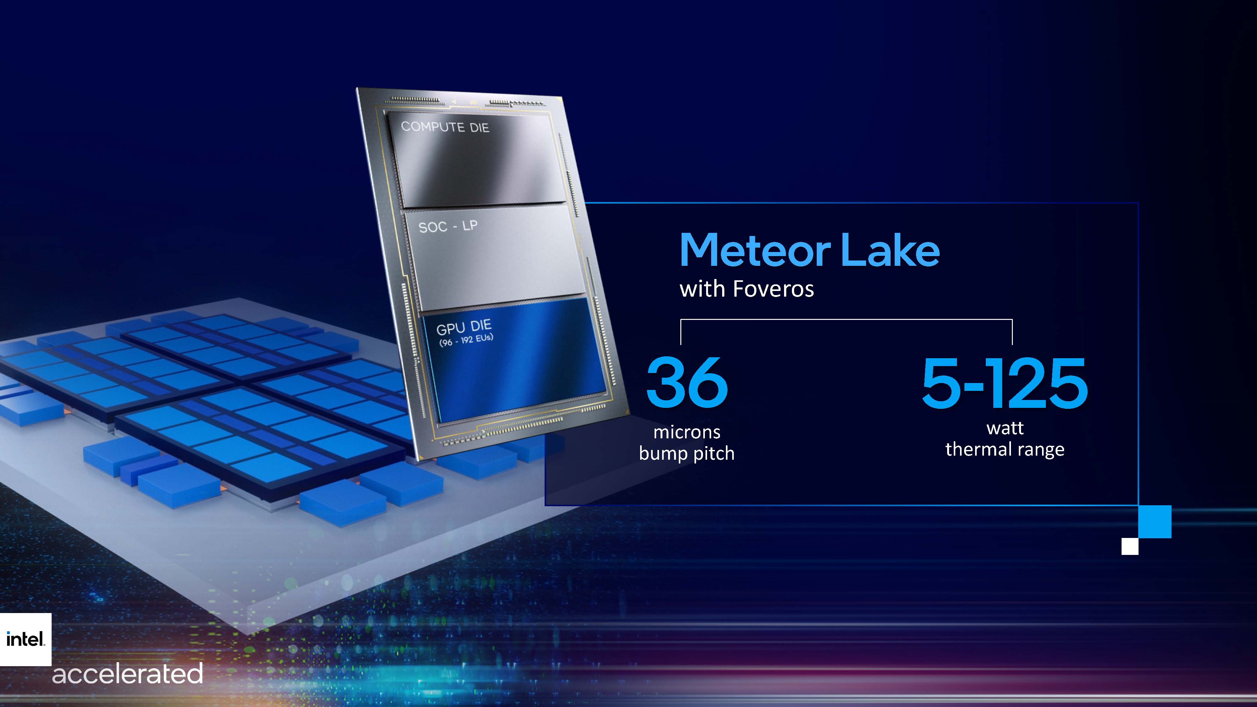
Meteor Lake processor will be Intel's first client PC CPU to adopt a multi-tile design with Foveros packaging technology: a compute die with an unknown number of Ocean Cove high-performance cores and energy-efficient Gracemont cores, a GPU die with 96 EUs – 192 EUs, and an SoC die packing such units as a memory controller, a PCIe controller, and a Thunderbolt controller. So far, Intel has only disclosed that Meteor Lake's compute die will be made using its own I4 fabrication process (previously known as 7 nm), whereas the SoC die will be produced using a low-power node.
It is noteworthy that Intel expects its Meteor Lake designs to scale from 5W to 125W, which suggests a very wide range of applications that these processors will be able to address, including traditional ones like tablets, notebooks, and desktops.
The chip is expected to use LGA 1700 or LGA 1800 packaging, but do not expect it to be compatible with LGA 1700 motherboards for Intel's 12th Generation Core 'Alder Lake' processors.
Get Tom's Hardware's best news and in-depth reviews, straight to your inbox.

Anton Shilov is a contributing writer at Tom’s Hardware. Over the past couple of decades, he has covered everything from CPUs and GPUs to supercomputers and from modern process technologies and latest fab tools to high-tech industry trends.
-
hotaru.hino Using "SoC" for what is essentially the I/O die threw me off, because it's not really an SoC by the standard definition of it, i.e., a CPU with most of the other things it needs to build a complete system around it.Reply
I was really hoping for something interesting like the I/O die containing the lower power cores. That way the Compute die can power off completely in extreme power saving modes.