Intel to Expand Arrow Lake's L2 Cache Capacity

Intel Meteor Lake
(Image credit: Intel)

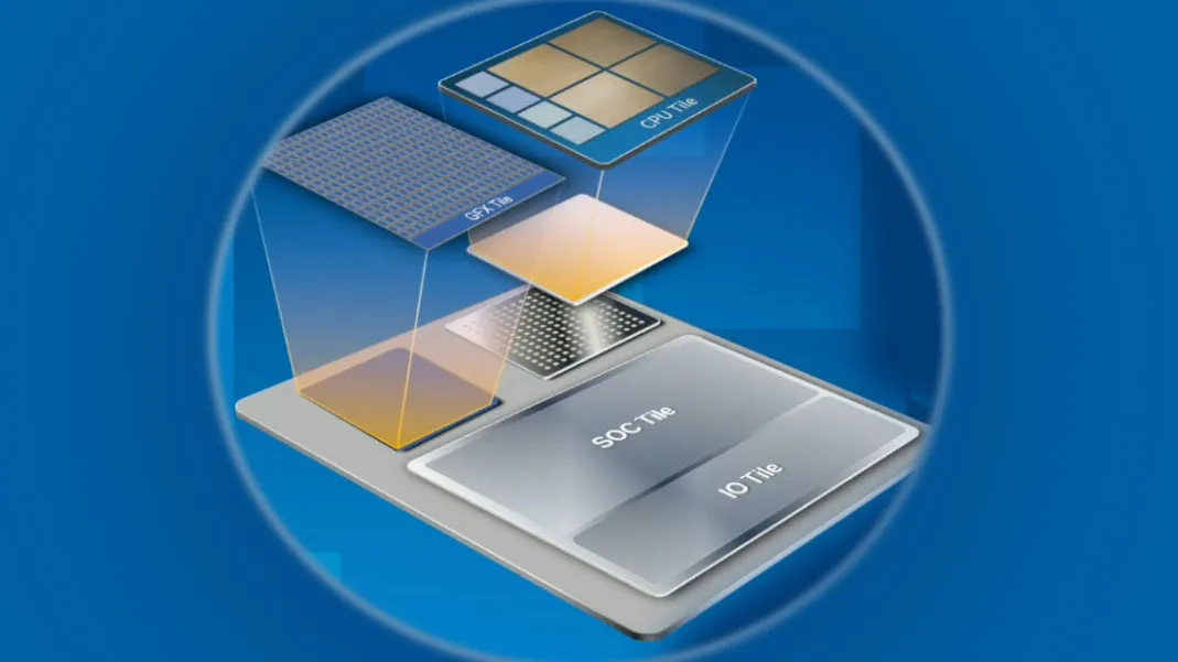
Intel intends to increase the L2 capacity of its upcoming codenamed Arrow Lake processors to 3 MB per core, according to Golden Pig Upgrade (via @9550pro), a renowned leaker who tends to have accurate information about future Intel products. If the information is accurate, then Arrow Lake CPUs will offer higher performance in memory bandwidth-dependent applications.

Intel's 13th Generation Core 'Raptor Lake' processor features a 2 MB L2 cache per high-performance Raptor Cove core and 512 KB L2 cache per energy-efficient Greacemont core, thus has 32 MB of L2 cache in total as well as 36 MB of L3 cache in total (3 MB L3 cache per P core, 3 MB per four E cores).

Swipe to scroll horizontally
Row 0 - Cell 0 P-CoreP-core L2E-CoreE-core L2
Alder LakeGolden Cove1.25 MBGracemont512 KB
Raptor LakeRaptor Cove2 MBGracemont512 KB
Meteor LakeRedwood Cove?Crestmont?
Arrow Lake?3 MBCrestmont?
Lunar LakeLion Cove?Skymont?

Assuming that Intel's Arrow Lake processors will retain eight high-performance cores, its total L2 capacity for performance cores will increase to a sizeable 24 MB. Meanwhile, it is unclear whether Intel also plans to expand the size of the L3 cache of Arrow Lake's performance cores. Keeping in mind that Arrow Lake CPUs will be made on Intel's 20A (2nm-class) fabrication process, the company might increase the size of all caches as it may not have a significant impact on die size and cost. Yet, only Intel knows what makes sense to do to increase performance without significantly affecting costs. 

(Image credit: Intel)

Increasing the L2 cache capacity for high-performance cores is done to boost performance. One of the primary benefits of increasing cache size is to improve the hit rate. If the working set of a given workload fits better within the enlarged L2 cache than it did before, this will reduce the need to access the slower L3 cache or main memory. This potentially leads to a reduction in average memory access time and potential energy savings, especially beneficial for workloads whose data sets can better fit within the enlarged L2 cache.

On the downside, a larger L2 cache can introduce slightly longer access latency. Keeping in mind that Intel's processors already have large L3 caches increasing L2 cache size gets diminishing returns on performance benefits. Additionally, a large L2 cache might consume more power, produce more heat, and increase die area. 

Anton Shilov
Freelance News Writer

Anton Shilov is a Freelance News Writer at Tom’s Hardware US. Over the past couple of decades, he has covered everything from CPUs and GPUs to supercomputers and from modern process technologies and latest fab tools to high-tech industry trends.

  • bit_user
    Keeping in mind that Arrow Lake CPUs will be made on Intel's 20A (2nm-class) fabrication process, the company might increase the size of all caches as it may not have a significant impact on die size and cost.
    Depends on what you're comparing against. Comparing "20A" against Intel 7, there might still be some significant margins for shrinking SRAM cells. However, we know SRAM is no longer scaling down well. So, I wouldn't assume it's "free", in terms of die area.
    Reply
  • TerryLaze
    bit_user said:
    Depends on what you're comparing against. Comparing "20A" against Intel 7, there might still be some significant margins for shrinking SRAM cells. However, we know SRAM is no longer scaling down well. So, I wouldn't assume it's "free", in terms of die area.
    Why did you feel compelled to write this up?!
    "As it may not have a significant impact" is not a synonym for free,
    so they didn't assume that it would be free and you just said that you would assume it to be free either, so what's your point here!?
    Reply
  • bit_user
    TerryLaze said:
    Why did you feel compelled to write this up?!
    "As it may not have a significant impact" is not a synonym for free,
    so they didn't assume that it would be free and you just said that you would assume it to be free either, so what's your point here!?
    The wording in the article diminishes the area-impact, which I felt wasn't appropriate, absent any data on SRAM scaling for the 20A node. Of all writers here, Anton should definitely be aware of that.
    https://www.tomshardware.com/news/no-sram-scaling-implies-on-more-expensive-cpus-and-gpus
    If you have said scaling data for Intel's 20A node, please provide it. If not, then you've failed to invalidate my calling the article's statement into question. Not helpful.
    Reply
  • TerryLaze
    bit_user said:
    The wording in the article diminishes the area-impact, which I felt wasn't appropriate, absent any data on SRAM scaling for the 20A node.

    If you have such data, please provide it. If not, then you've failed to invalidate my calling the article's statement into question. Not helpful.
    Diminishing means to make less not to make non existent, it still has nothing to do with free.
    Reply
  • InvalidError
    bit_user said:
    Depends on what you're comparing against. Comparing "20A" against Intel 7, there might still be some significant margins for shrinking SRAM cells. However, we know SRAM is no longer scaling down well. So, I wouldn't assume it's "free", in terms of die area.
    Since SRAM memory arrays have pretty low power density, that would be one place where CPU and GPU designers should be able to easily stack CMOS ribbons at least two-high to make SRAM cells with a ~3T planar footprint. There should be a one-time rough doubling of SRAM density to be had there, more if they stack more active layers further down the line to the point of being able to stack SRAM bits.
    Reply
  • bit_user
    InvalidError said:
    Since SRAM memory arrays have pretty low power density, that would be one place where CPU and GPU designers should be able to easily stack CMOS ribbons at least two-high to make SRAM cells with a ~3T planar footprint. There should be a one-time rough doubling of SRAM density to be had there, more if they stack more active layers further down the line to the point of being able to stack SRAM bits.
    Could Intel's 20A process enable such techniques without Intel having touted it, in their public announcements about it and 18A? I rather doubt that. These are effectively sales pitches by IFS, to try and lure fab customers. Such an increase in SRAM density would be a big selling-point.

    Or, are you simply pointing out that they could do this sort of thing in some future node or iteration?
    Reply
  • InvalidError
    bit_user said:
    Or, are you simply pointing out that they could do this sort of thing in some future node or iteration?
    If you have the ability to do ribbon FETs, you have the ability to dope an arbitrary number of layers an arbitrary distance from the base silicon, which means the ability to stack CMOS too. From there, it is only a matter of being able to achieve sufficient yields doing so and also having the incentive to actually do it.
    Reply
  • bit_user
    InvalidError said:
    If you have the ability to do ribbon FETs, you have the ability to dope an arbitrary number of layers an arbitrary distance from the base silicon, which means the ability to stack CMOS too. From there, it is only a matter of being able to achieve sufficient yields doing so and also having the incentive to actually do it.
    Sounds cool, but I think:
    The fab node would need to actually incorporate the extra layers to do it. More layers increases cost and shouldn't help yields, either.
    They would probably need to provide these cells in their cell library.
    Which is to say I think it won't sneak up as some sort of Easter egg, but rather will probably come along as an iterative refinement on one of their GAA nodes.
    Reply
  • ThisIsMe
    Even if there is no significant increase in sram density on the new process node there will likely still be some improvements. There will also be significant improvements in logic density likely freeing up die area, so a mere 50% increase in L2 cache size is plausible. Regardless, the increase would still be enabled by density improvements.

    As for the other concerns, the additional performance benefits of the newer node may also allow for an L2 cache performance boost even after the performance costs of the size increase. It’s of course all speculation, but it’s hard to imagine intel backtracking on cache performance.
    Reply
  • Nicholas Steel
    Meanwhile, it is unclear whether Intel also plans to expand the size of the L3 cache of Arrow Lake's performance cores.
    I believe you meant Efficiency Cores in this sentence.
    Reply