When Japan and the U.S. announced joint development of a 2nm fabrication technology earlier this year, we were skeptical. But as it turns out, the Japanese government is very serious about the project, and it plans to allocate some ¥350 billion (nearly $2.38 billion) to build the joint research hub with the U.S.
The research hub will be comprised of Japanese and American semiconductor companies that are yet to be named, as well as multiple universities from Japan, the U.S. and Europe, reports Nikkei. Among the Japanese universities, the business publication names the University of Tokyo, the National Institute of Advanced Industrial Science and Technology, and Riken. IBM is also said to be among the candidates to participate.
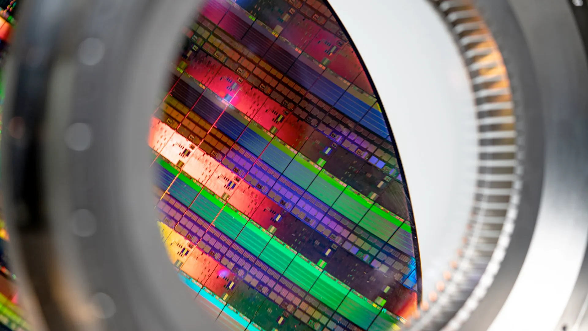
The hub will conduct fundamental research to explore materials needed to make chips using a 2nm-class fabrication technology by the latter half of the decade. But it's is unclear whether Japan has plans to build actual fabs that will make commercial chips. And if such plans exist it is unclear which of the Japanese companies have enough money and scale to make chips on a leading-edge node.
It has been quite a while when Japanese companies were leaders of the microelectronics market. Today, only Kioxia produces leading-edge memory in Japan. Other Japanese chip developers either use trailing nodes to make their products domestically, or outsource their production to Taiwan Semiconductor Manufacturing Co (TSMC).
But the Japanese government wants to revive the country's semiconductor industry, which is why it approved subsidies for Kioxia and Western Digital, Micron, and TSMC to build new fabs in the country.
In addition to spending ¥350 billion ($2.38 billion) on the new research hub, the Japanese government also intends to spend ¥450 billion ($3.071 billion) on advanced production hubs, as well as ¥370 billion ($2.525 billion) on securing materials required for manufacturing, which emphasizes how serious the authorities in Japan are about the chip industry.
