Micron Secures $320 Million in Japanese Subsidies, Might Bring EUV to Japan
Micron to get subsidies from Japan as it cuts CapEx for fiscal 2023.
Having understood the importance of the local semiconductor supply chain for long-term homegrown microelectronics industry development, the Japanese government kicked off a program to subsidize local chipmakers. On the heels of its $680 million subsidy for Kioxia and Western Digital in July, the Japanese govt announced plans to support Micron's Hiroshima operations with ¥46.5 billion ($320 million). This cash infusion might help Micron bring extreme ultraviolet (EUV) lithography to Japan.
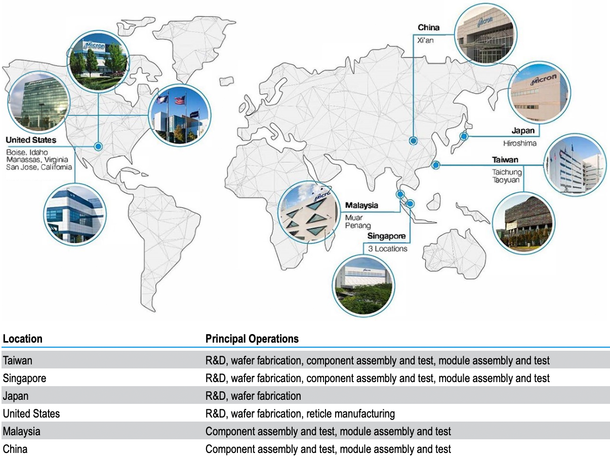
Micron will receive the funding from Japan's Ministry of Economy, Trade and Industry, reports Bloomberg. However, the conditions that Micron must meet to get the subsidy were unavailable via the ministry's website at the time of writing. The grant will help Micron 'mass produce cutting-edge memory chips' at its fabs near Hiroshima, Japan, which the company obtained when it acquired Elpida in 2013.
Micron produces a significant portion of its DRAM products at its site near Hiroshima, Japan, and runs important R&D operations in the country. To keep DRAM fabs up-to-date, Micron and other memory makers must constantly install new equipment to adopt new manufacturing technologies and increase capacity, which requires hefty investments. Since capital expenditures (CapEx) are getting extremely high in the semiconductor industry these days, chipmakers like Micron are seeking support and incentives from governments. They plan their own spending based on what they might receive in grants and various enticements.
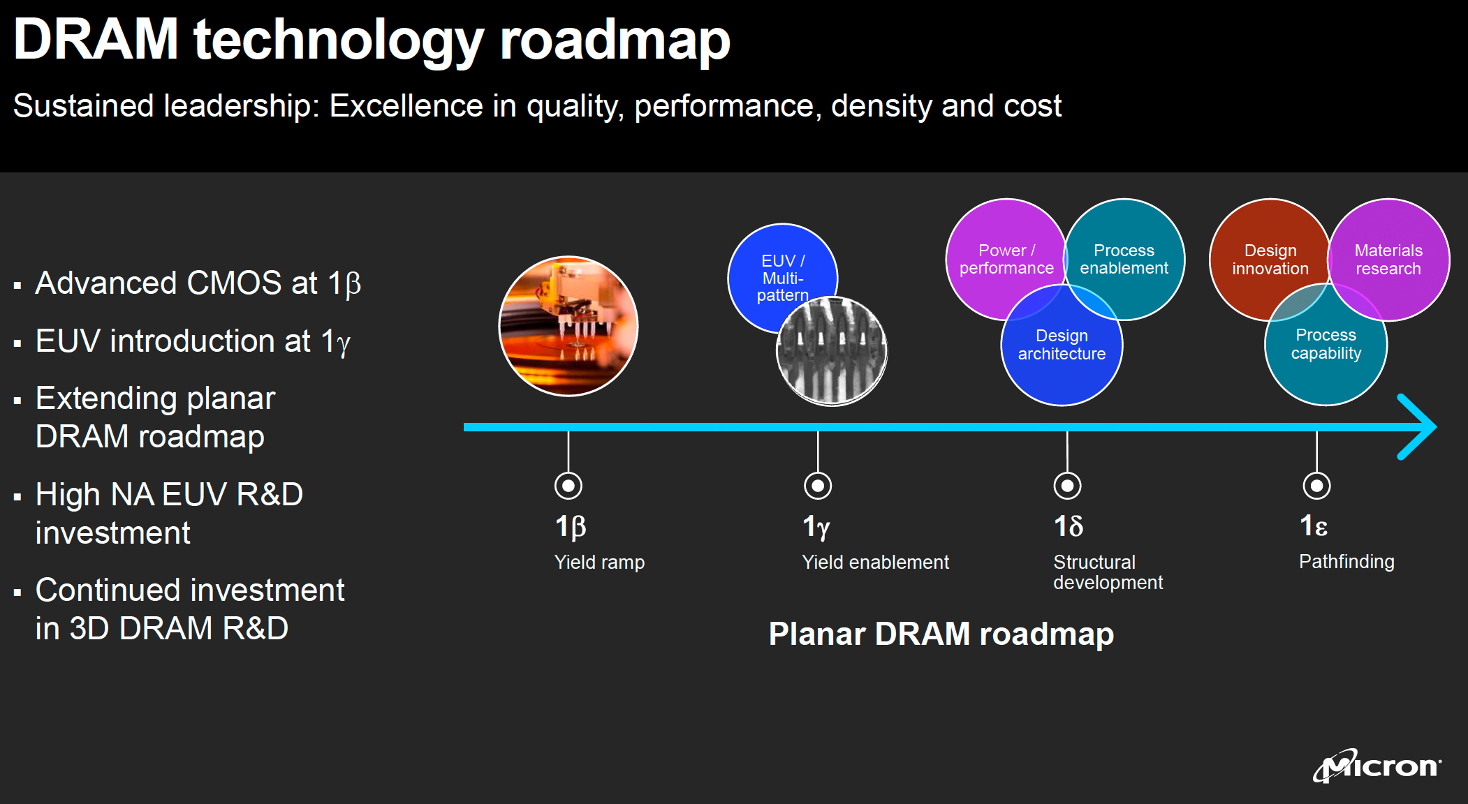
$320 million is a lot of money, though it remains to be seen how much money Micron will be willing to spend on Hiroshima site expansion. Just yesterday, the company said that it cut down its fiscal year 2023 CapEx budget by 30% year-over-year to around $8 billion. To reduce its capital expenditures, the company trimmed its wafer fab equipment (WFE) CapEx by nearly 50% YoY, which will result in a much slower ramp of its 1ß DRAM and 232-layer 3D NAND versus prior expectations as the ramp requires more new tools at the fabs. Meanwhile, the company "more than doubled" its construction CapEx (i.e., building new fab shells) year-over-year to meet demand for the second half of this decade and retained plans to procure EUV lithography systems to support its 1γ (1-gamma) node development.
The $320 million subsidy from the Japanese government could be used to bolster the Hiroshima site's WFE CapEx budget to ramp up 1ß DRAM node in Japan next year or procure new EUV tools and ramp up EUV-enabled 1γ DRAM fabrication technology in Japan sometime in 2024. Keeping in mind that many things for 1ß DRAM manufacturing process should be arranged by now (i.e., which tools go where), the grant might indeed be used for the next round of Micron's Hiroshima site expansion, the one that involves ASML's EUV scanners and the company's 1γ DRAM.
For now, we have more questions than answers, but it looks like the subsidy from the Japanese government comes at a time when Micron is slowing down upgrades of its current fabs by cutting down its WFE CapEx.
Get Tom's Hardware's best news and in-depth reviews, straight to your inbox.

Anton Shilov is a contributing writer at Tom’s Hardware. Over the past couple of decades, he has covered everything from CPUs and GPUs to supercomputers and from modern process technologies and latest fab tools to high-tech industry trends.
-
RedBear87 In 1986 Japan was forced to limit its export of semiconductors by the US because of Japan's supposedly "unfair" competition, now Japan pays American semiconductor companies to expand their facilities there, sic transit gloria mundi...Reply -
jkflipflop98 $350M will get you one litho tool and the associated track. I guess it's better than nothing!Reply

