
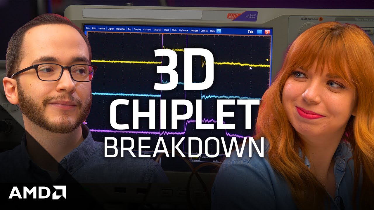
AMD's announcement of its new 3D V-Cache chip stacking technology for Ryzen processors was easily the most surprising announcement for PC enthusiasts at Computex 2021, and today the company has shared a few more details via its YouTube program The Bring Up, which you can see embedded below.
The high-level 3D V-Cache overview is that AMD has 3D-stacked chiplets for the Zen 3 architecture that will go into production this year. These innovative new chiplets feature an additional 64MB of 7nm SRAM cache (called 3D V-Cache) stacked vertically atop the core complex die (CCD) to triple the L3 cache for the CPU cores.
At Computex, AMD CEO Lisa Su shared a broad overview of the tech — it enables up to a whopping 192MB of L3 cache on a single Ryzen chip, which delivers up to a 15% improvement in gaming. Su also showed a prototype Ryzen 9 5900X chip that the company already has up and running and provided a pretty impressive demo of accelerated gameplay due to the new architecture.
We followed up with AMD, and the company confirmed that Zen 3 Ryzen processors with 3D V-Cache would enter production later this year. The technology currently consists of a single layer of stacked L3 cache, but the underlying tech supports stacking multiple dies. The technology also doesn't require any specific software optimizations and should be transparent in terms of latency and thermals (no significant overhead in either).
AMD's 3D chip stacking tech is based on TSMC's SoIC technology. The video above shares a few interesting details. AMD flips the die then shaves the standard compute die down by 95%, leaving only 20 micrometers of active silicon for compute purposes, which is thinner than a strand of human hair. AMD then places a standard L3 chip on top to complete the stack.
As we already know, TSMC's SoIC is a bumpless chip stacking tech, meaning that it doesn't use microbumps or solder to connect the two die. Instead, the two die are milled to such a perfectly flat surface that the TSV channels can mate without any type of bonding material, reducing the distance between the cache and core by 1000X. That reduces heat and power consumption while boosting bandwidth.
The video has many more details and goes into an explainer about chip interconnect technology, which is quite interesting and informative, along with a few more details about AMD's new stacking technique. Give it a watch.
