Nvidia Details Volta GV100 GPU, Tesla V100 Accelerator
Get Tom's Hardware's best news and in-depth reviews, straight to your inbox.
You are now subscribed
Your newsletter sign-up was successful
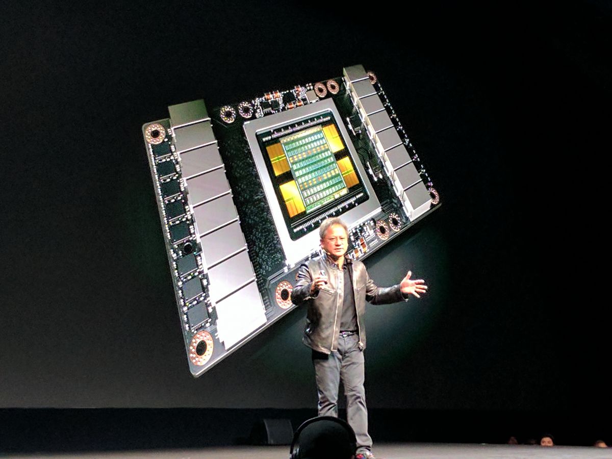
Nvidia pulled back part of the curtain to reveal its long-anticipated Volta GPU architecture, showing the GV100 GPU and the first derivative product, the Tesla V100, here at GTC in San Jose. Nvidia first dropped the Volta name at GTC in 2013, and it's taken the company four years to get to the juicy details. If you're a gamer, don't get too excited yet, though; Nvidia is still pitching Pascal-derived products (only a year old, or less) for you. If you work in the AI and high performance computer (HPC) markets, however, this first phase of Volta is coming your way.
The Volta GV100 GPU Architecture
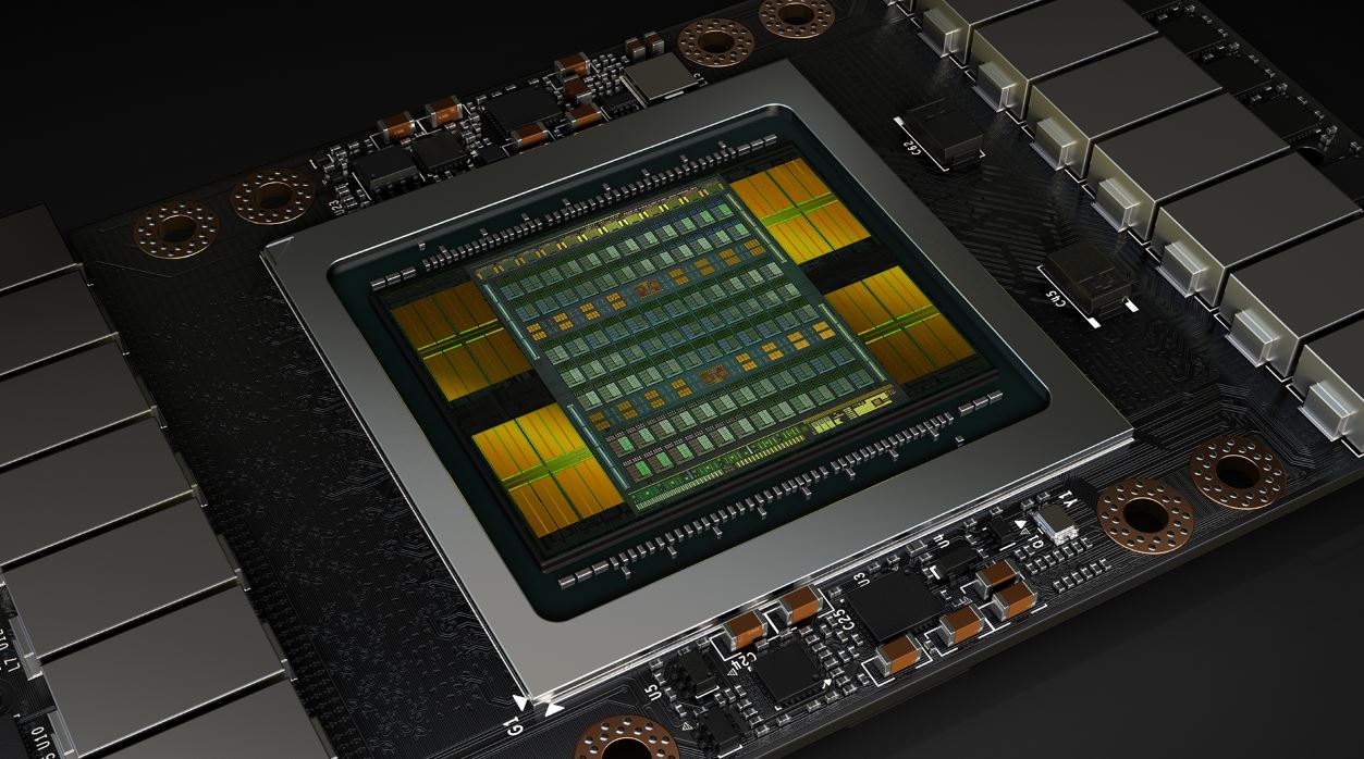
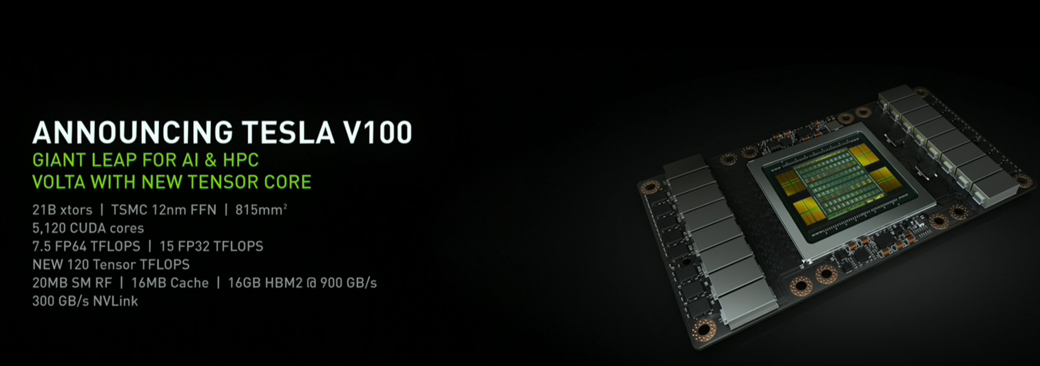
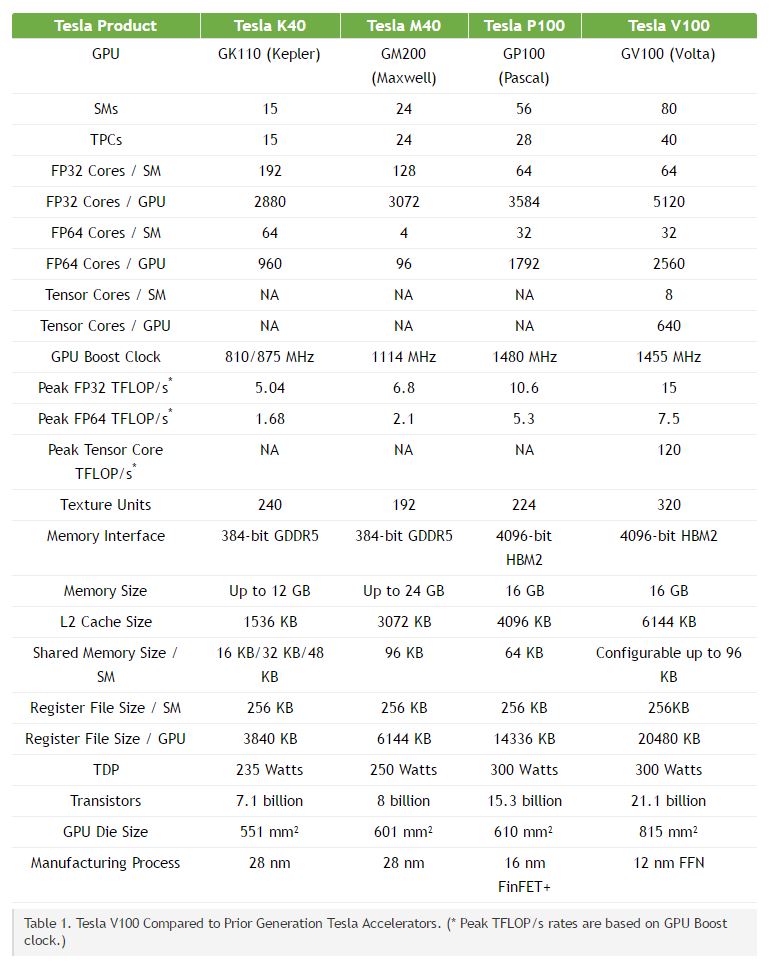
The Volta GV100 GPU uses the 12nm TSMC FFN process, has over 21 billion transistors, and is designed for deep learning applications. We're talking about an 815mm2 die here, which pushes the limits of TSMC's current capabilities. Nvidia said it's not possible to build a larger GPU on the current process technology. The GP100 was the largest GPU that Nvidia ever produced before the GV100. It took up a 610mm2 surface area and housed 15.3 billion transistors. The GV100 is more than 30% larger.
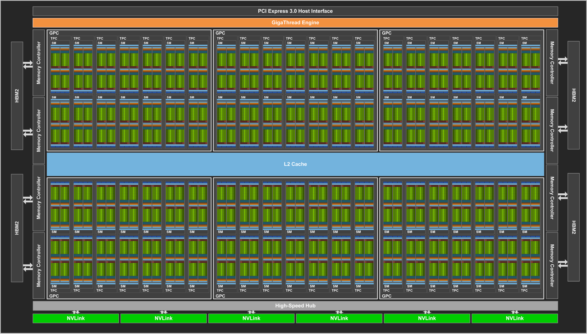
Volta’s full GV100 GPU sports 84 SMs (each SM features four texture units, 64 FP32 cores, 64 INT32 cores, 32 FP64 cores) fed by 128KB of shared L1 cache per SM that can be configured to varying texture cache and shared memory ratios. The GP100 featured 60 SMs and a total of 3,840 CUDA cores. The Volta SMs also feature a new type of core that specializes in Tensor deep learning 4x4 Matrix operations. The GV100 contains eight Tensor cores per SM and deliver a total of 120 TFLOPS for training and inference operations. To save you some math, this brings the full GV100 GPU to an impressive 5,376 FP32 and INT32 cores, 2688 FP64 cores, and 336 texture units.
Article continues belowLike the GP100, we get two SMs per TPC; 42 TPC overall in the GV100. And that rolls up into six GPCs.
GV100 also features four HBM2 memory emplacements, like the GP100, with each stack controlled by a pair of memory controllers. Speaking of which, there are eight 512-bit memory controllers (giving this GPU a total memory bus width of 4,096-bit). Each memory controller is attached to 768KB of L2 cache, for a total of 6MB of L2 cache (vs 4MB for Pascal).
Tesla V100
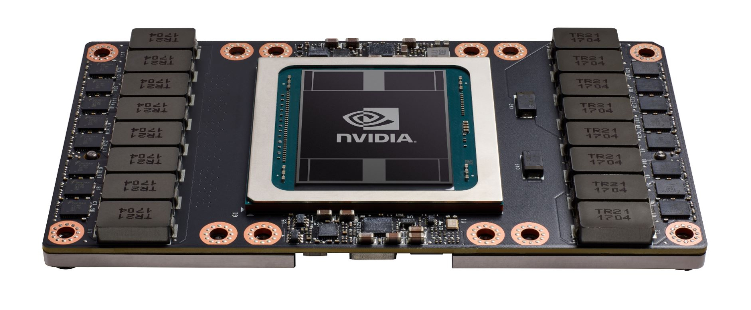
The new Nvidia Tesla V100 features 80 SMs for a total of 5,120 CUDA cores. However, it has the potential to reach 7.5, 15, and 120 TFLOPs in FP64, FP32, and Tensor computations, respectively.
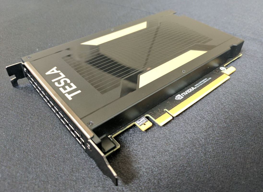
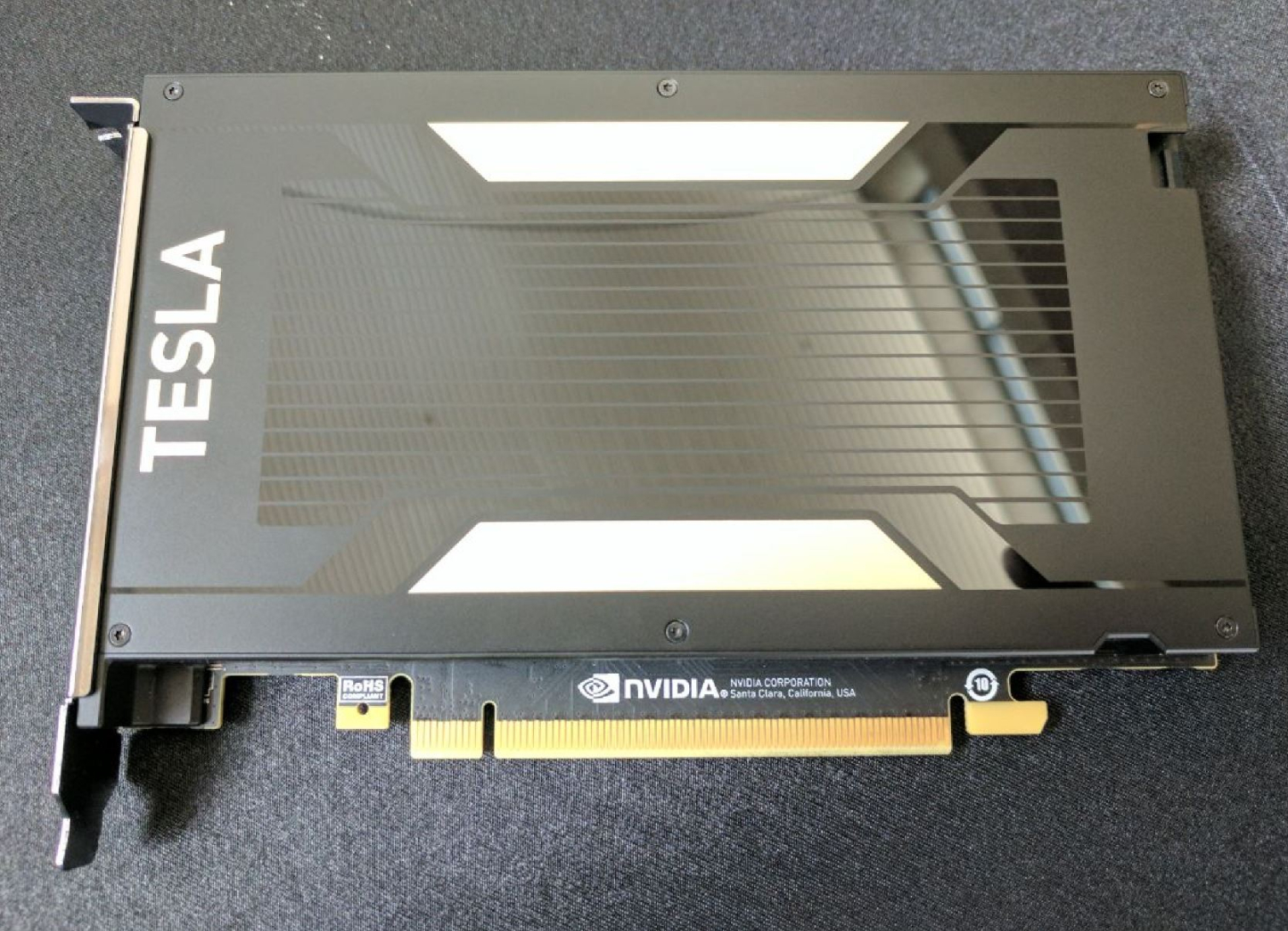
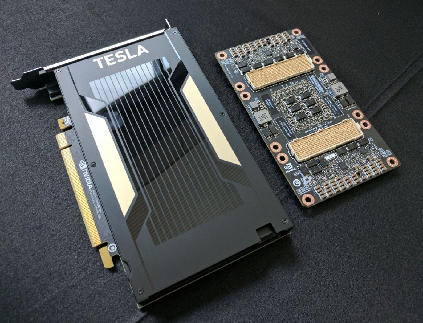
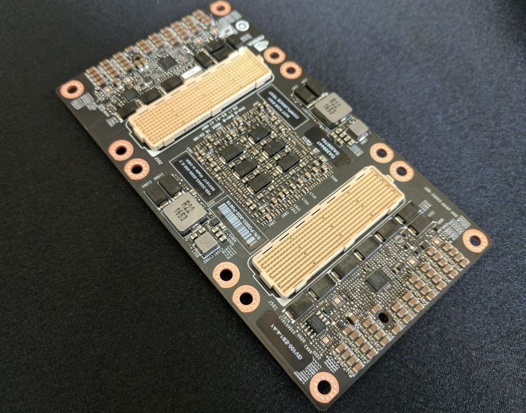
The Tesla V100 sports 16GB of HBM2 memory, which is capable of reaching up to 900 GB/s. The Samsung memory that Nvidia installed on the Tesla V100 is also 180 GB/s faster than the memory found on the Tesla P100 cards. Nvidia said it used the fastest memory available on the market.
Get Tom's Hardware's best news and in-depth reviews, straight to your inbox.
The Tesla V100 also introduces the second generation of NVLink, which allows for up to 300 GB/s over six 25 GB/s NVLinks per GPU.
To put those numbers into perspective, Nvidia's Pascal-derived Tesla P100 sports 56 SMs and 3,584 CUDA cores, which produce up to 5.3 TFLPs in FP64 computations, and 10.6 TFLOPs in FP32 computations. The V100 offers a full 30% more FP32 computational capability than the P100, and nearly a 50% increase in FP64 performance. And Nvidia increased the NVLink bandwidth of the Tesla V100 by 50% by adding two NVLinks per GPU compared to the Tesla P100, and by increasing the bandwidth of each NVLink by 5GB/s.
Nvidia said the Tesla V100 carries a TDP of 300W, which is the same power requirement as the Tesla P100.
| Header Cell - Column 0 | V100 | P100 |
|---|---|---|
| SMs | 80 | 56 |
| Cores | - 5,120 (FP32)- 2,560 (FP64) | - 3,584 (FP32) - 1,792 (FP64) |
| Boost Clock | 1,455MHz | 1,480MHz |
| TFLOPs | - 7.5 (FP64)- 15 (FP32)- 120 Tensor | - 5.3 (FP64) - 10.3 (FP32) |
| Texture Units | 320 | 224 |
| Memory | 16GB 4096-bit HBM2 | 16GB 4096-bit HBM2 |
| Data Rate | 900 GB/s | 720 GB/s |
| Transistors | 21.1 Billion | 15.3 Billion |
| Manufacturing Process | 12nm FFN | 16nm FinFET+ |
Derek Forrest was a contributing freelance writer for Tom's Hardware. He covered hardware news and reviews, focusing on gaming desktops and laptops.
-
bit_user ReplyThe GV100 contains eight Tensor cores per SM, and each core delivers up to 120 TFLOPS
That can't be right.
Each tensor core generates 64 FMAs per clock, translating to 128 FLOPs. At 8 tensor cores per SM, you get 1024 FLOPs per SM, which works out to 1 TFLOPS @ 1 GHz. Now, if we assume it was 120 TFLOPS for the entire GPU, then that would yield a very reasonable clock speed of 1.43 GHz, assuming all 84 SMs were enabled, or 1.5 GHz assuming 80 SMs.
That's awfully impressive. I'd bet we're not talking about IEEE 754-compliant floating point, here. They must've cut some things besides denormals to get that much speed up over their normal SIMD units.
second generation of NVLink ... allows for up to 300 GB/s over six 25GB/s NVLinks per GPU.
Because it's bidir, and they're counting each direction. -
Paul Alcorn Reply19675100 said:each core delivers up to 120 TFLOPS
That can't be right.
Each tensor core generates 64 FMAs per clock, translating to 128 FLOPs. At 8 tensor cores per SM, you get 1024 FLOPs per SM, which works out to 1 TFLOPS @ 1 GHz. Now, if we assume it was 120 TFLOPS for the entire GPU, then that would yield a very reasonable clock speed of 1.43 GHz, assuming all 84 SMs were enabled.
You're right, it's 120 peak Tensor core TFLOPs for the total card. With the caveat that Peak TFLOP/s rates are based on GPU Boost clock. Fixed :)
-
bit_user BTW, it sounds like there are some interesting efficiency enhancements, in the form of sub-warp granularity scheduling. Anandtech hinted at this (pretty explicitly, I might add), but said that details would have to wait.Reply
I'm guessing there are probably specific synchronization points at which warps can get broken up & reconstituted. It's not going to be fully-independent scheduling of each lane, or else it'd no longer be "Single Instruction", with its attendant benefits. -
redgarl So basically 15 TFLOP FP32... of course if you are putting many chips together that number will go up 15X8 = 120...Reply
Why not 15 X 1000 = 15 000 WOW.... cmon... seriously? -
JackNaylorPE Reply19675649 said:But does it has RGB?
Ahhh ... you beat me to it :0
This comes on the back of a video i just watched entitled "if this is what the new iPhone, looks like, Samsung is in trouble". With the younger generations allegedly being "tech savvy", this obvious bent towards from over function proves that "tech savvy" assumption blatantly wrong. How about a smartphone for which I don't have to say "Let me call you back from a land-line" ? How about a phone that doesn't focus on form giving me the thickness of a slice of cheese and batterly life less than a day, and instead gives me a week of battery life, as my Treo 650 did more than 12 years ago ? Give it 3 months ... then the fad that says t says "I'm in the know, I'm not a bling bling guy" will be the total absence of RGB. I have watched me kids go thru ...
I wanna see Britney Spears concert ... I would not be caught dead at a Britney Spears concert
I gotta have an iPhone ... I gotta have anything but an iPhone
Today, my kids and their peers have aged out of the fad thing (oldest approaching 30) but, those peers with younger siblings it's.... I gotta have bling bling up the gazoo .... mark my words :)
-
bit_user Reply
That math only works by coincidence. The 120 TFLOPS number is derived according to my post, above. On a related note, the TPU uses fp16. Since they didn't quote another fp16 number, it might've replaced the double-rate fp16 support in P100.19676419 said:So basically 15 TFLOP FP32... of course if you are putting many chips together that number will go up 15X8 = 120...
BTW, I was surprised not to see anything about int8 performance. -
bit_user Reply
Your "old man" is showing. Seriously, what does that have to do with this?19676737 said:With the younger generations allegedly being "tech savvy",
And yes, I think significantly more kids in this generation are meaningfully tech-savvy than previous generations. I'd actually find it pretty intimidating if the majority were actually nerds like us.
-
Stormfire962 So how much is this card going to cost us consumers? A whopping $1,000 USD or a more reasonable price like $350 USD and will it be true to NVidia word which is not worth much today since they have lied to the customer in the passed! Frankly I am getting pretty damn tired of NVidia boasting a lot and not delivering on their so call promises. They told us SLI was the way of the future and that failed. They lied about the memory specs of the 900 series and got caught doing it. Now they are coming out with another so call super graphics card? I cannot help to wonder how long they had this sitting on their shelf holding off to release it just to sucker us consumers yet again.Reply
Sorry all for the nasty response. But I think NVidia has lost their focus on doing right by us consumers and are focusing more on making a quick buck and damn us all again.
