Samsung Prototypes First Ever 3nm GAAFET Semiconductor
5nm isn't publically available yet, but Samsung is already making big steps in the 3nm space.

The 7nm process is reaching its peak. Nvidia's rumored to start placing orders at TSMC and Samsung for releasing its next-generation 'Ampere' graphics cards mid-2020. Meanwhile, we already know that TSMC is investing heavily in 5nm fabrication, with Apple purportedly having reserved two-thirds of TSMC's 5nm capacity for the A14 SoC expected to power the iPhone 12.
Now, Samsung has succeeded in making the first strides towards the 3nm process, as reported by the Korean Maeil Economy this week. According to the report, Samsung's goal is to become the world's number one semiconductor manufacturer by 2030.
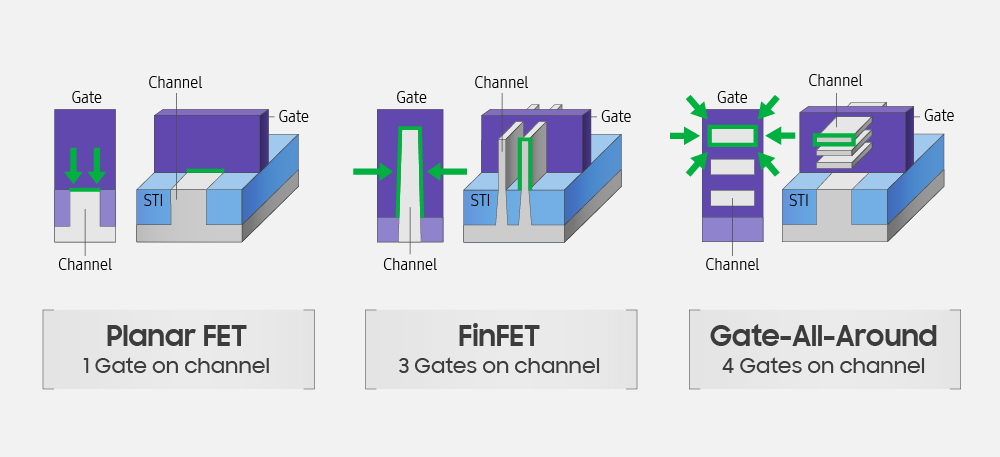
Samsung's work on the 3nm process is based on the Gate All Around (GAAFET) technology rather than FinFET. This supposedly reduces the total silicon size by 35% while using about 50% less power and allows for the same amount of power consumption and 33% performance increase over the 5nm FinFET process.
Article continues belowWe first heard that Samsung was working on the 3nm GAAFET process a year ago, when it said that it targeted mass production in 2021. That was considered ambitious at the time, but if Samsung has already succeeded in producing its first 3nm prototypes, the vendor might be closer than expected.
The GAAFET design differs from the FinFET design in that it is built around having gates around four sides of the channel, which ensures reduced power leakage and thus improved control over the channel -- a fundamental step when shrinking the process node. This switch to a more efficient transistor design paired with the decreased node size is what enables the tremendous jump in performance per watt over a 5nm FinFET process.
Get Tom's Hardware's best news and in-depth reviews, straight to your inbox.
Niels Broekhuijsen is a Contributing Writer for Tom's Hardware US. He reviews cases, water cooling and pc builds.
-
12pak Out of curiosity, how are these tech companies getting past the 7nm barrier? Several years back, when we were anxiously awaiting the 14nm technology, I remember reading that science would hit a wall at 7nm due to that mathematically being the smallest reachable size without melting the transistor, unless a new material was found to replace silicone. Now I don't claim to understand that, but I do remember reading it.Reply
Between then and now, what happened that allowed them to break that barrier? -
JamesSneed Reply12pak said:Out of curiosity, how are these tech companies getting past the 7nm barrier? Several years back, when we were anxiously awaiting the 14nm technology, I remember reading that science would hit a wall at 7nm due to that mathematically being the smallest reachable size without melting the transistor, unless a new material was found to replace silicone. Now I don't claim to understand that, but I do remember reading it.
Between then and now, what happened that allowed them to break that barrier?
The light was the main issue for getting to 7nm so they are using EUV. Well TSMC's first 7nm node is using quad patterning(think like using a stencil to spray paint letters but you have to apply 4 times) but it's not that great. There next node is using EUV which is what iPhone APU's are made with. They can use traditional FinFET designs and extreme ultraviolet light to get down to 5nm. After that they have to use this gate all around approach which involves all sorts of tech like nano wires. You can think of CPU designs going 3d so to speak to overcome these physical limitations. What this does is give a contact area that is larger than the smallest feature sizes so you don't run into physical limits.
The photo in the article should help visualize. -
JamesSneed The densities are going to be insane. Having APU's that can really play games is going to be possible. The efficiencies should be pretty cool for phones as well. The only thing I haven't seen much about is the frequencies which is what concerns me the most.Reply -
CerianK Reply
That should not be too much of a concern, as the worst case hit I have read for 3-5nm is 20%, which they should be able to erase through normal process node optimization and (for CPUs) IPC improvements with the more advanced architectures enabled by the increased density.JamesSneed said:... The only thing I haven't seen much about is the frequencies which is what concerns me the most.
Eventually head-room may run out with existing materials (and assuming no cost-effective advancement with new materials), it may be possible to push frequency up by using more fault-tolerant and/or redundant designs. This is already the status-quo with ECC DRAM and cutting-edge quantum electronics, etc., so at least there is some precedent to guess all will be well down to 1-1.5nm. Below that, I don't think there is enough information currently available to speculate what is cost-effectively possible. -
JamesSneed @Cerian No argument on what you said mostly I am wondering out loud how that will slow down progress. I have a feeling frequency is going to be a hard one for high performance parts like desktop and server CPU's. It may be overcome quickly but I have some doubts on how long it will take.Reply -
JordonB It has to do with electron tunneling through the insulators when the conductive areas get too small. Different methods like Intels tri-gates have helped. I do not know what the secret sauce is for 7 and below but its all about making electrons behave.Reply -
alextheblue Reply
I mean that's already happened... 5 TFLOPs is pretty decent. If you strictly mean standard consumer APUs, they'll improve, but so will dGPUs. Developers will in turn seek to harness varying degrees of this extra horsepower. So it's hard to predict if they'll get much further than the current esports / less demanding games / older games capability. I think a lot of that depends on how aggressive Intel gets with their iGPUs, as competition will be crucial to more rapid improvements on the graphics side of APUs.JamesSneed said:The densities are going to be insane. Having APU's that can really play games is going to be possible. -
CerianK Reply
Not long. I just bumped into an apparent CPU architectural improvement recently regarding the performance of the load effective address instruction on x86/x64. Apparently the latency of the compound adder was reduced and compilers have already been rewritten to take it advantage of it in general purpose summing for better pipeline parallelization of normal code. The combination of hardware and software optimization should prevent the release of any new architectures where an IPC regression would actually occur... but we may have to get used to no more than 5% IPC improvement per generation below 7 mm.JamesSneed said:It may be overcome quickly but I have some doubts on how long it will take. -
ariliquin The change is in the equipment and methods used for the Lithography in the chip manufacturing. The "resolution" is greatly increased in EUV (Extreme Ultraviolet Lithography) over traditional processes. However there are significant hurdles to reduce impacts from dust. TSMC is leading at the moment as they use a patented curtain-less process on their EUV unlike Intel who is struggling to be able to manufacture at high enough yields. Not sure what Intel and Samsung is doing to overcome the challenges in EUV . I think all three manufacturers use the same EUV equipment manufactured in Europe.Reply
https://en.wikipedia.org/wiki/Extreme_ultraviolet_lithography
12pak said:Out of curiosity, how are these tech companies getting past the 7nm barrier? Several years back, when we were anxiously awaiting the 14nm technology, I remember reading that science would hit a wall at 7nm due to that mathematically being the smallest reachable size without melting the transistor, unless a new material was found to replace silicone. Now I don't claim to understand that, but I do remember reading it.
Between then and now, what happened that allowed them to break that barrier?

