Samsung Says 300+ Layer V-NAND is On Track for 2024
Samsung reiterates big plans for non-volatile memory

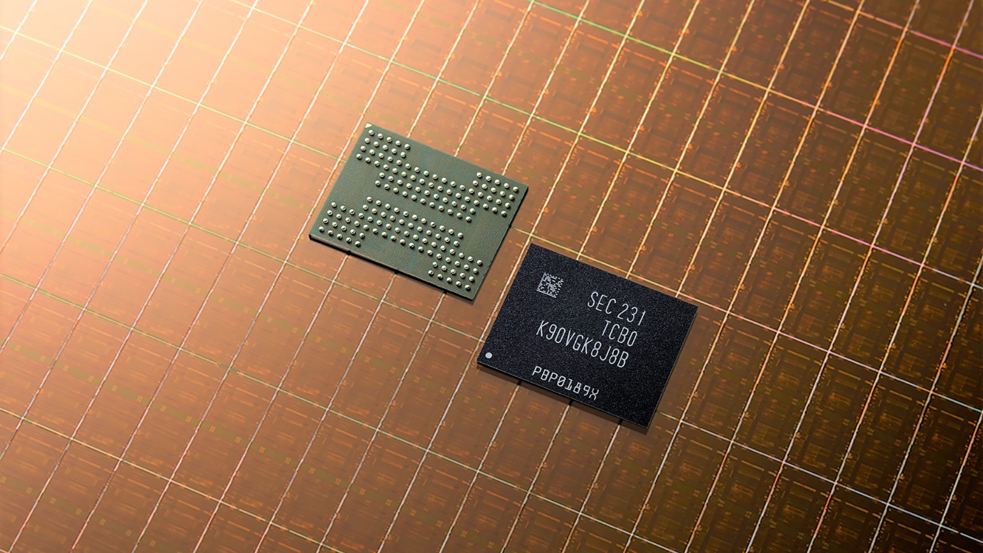
As the world's largest supplier of NAND memory, Samsung has big plans for development of its V-NAND (which is what the company calls its 3D NAND) — some of which it shared this week. The company confirmed that it is on-track to produce its 9th Generation V-NAND memory with over 300 layers in 2024 and said that it will have the highest number of active layers in the industry.
"The ninth-generation V-NAND is well under way for mass production early next year with the industry's highest layer count based on a double-stack structure," Jung-Bae Lee, President and Head of Memory Business at Samsung Electronics, wrote in a blog post.
We learned in August that Samsung was working on 9th Generation V-NAND with over 300 layers, which will retain the double-stacking technology first embraced by Samsung in 2020. Samsung not only confirmed that it's on-track with its next-generation non-volatile memory, but also that it will allegedly have more active layers than 3D NAND memory from competitors. So far we know that SK Hynix's next-gen 3D NAND will feature 321 active layers, so it appears that Samsung expects its memory to have more.
The increased number of layers will enable Samsung to increase storage density of its 3D NAND devices. The company expects upcoming types of flash memory not only to gain storage density, but also performance.
"Samsung is also working on the next generation of value-creating technologies, including a new structure that maximizes V-NAND's input/output (I/O) speed," said Jung-Bae Lee.
We do not know what we can expect from Samsung's 9th Generation V-NAND in terms of performance, though we're sure that the company will use this memory for its upcoming SSDs. Perhaps this is when we'll see the company's retail SSDs with a PCIe Gen5 interface — the successors to Samsung's 990 Pro series, which are currently among the best SSDs.
As far as longer-term technological innovation is concerned, Samsung is committed to minimizing cell interference, reducing height, and maximizing vertical layer count, which will enable it to attain the smallest cell sizes in the industry. These innovations will be instrumental in driving Samsung's vision of creating 3D NAND with over 1000 layers as well as highly differentiated memory solutions, and in ensuring that the company's offerings remain relevant for datacenters, PCs, and other applications.
Get Tom's Hardware's best news and in-depth reviews, straight to your inbox.

Anton Shilov is a contributing writer at Tom’s Hardware. Over the past couple of decades, he has covered everything from CPUs and GPUs to supercomputers and from modern process technologies and latest fab tools to high-tech industry trends.
-
Alvar "Miles" Udell Whatever happened to that supposedly industry changing XNAND?Reply
https://www.tomshardware.com/news/new-x-nand-tech-detailed-slc-speed-at-qlc-density-and-cost