Samsung to Produce 300-Layer V-NAND in 2024: Report
First details about Samsung's 300-layer 3D NAND leak.

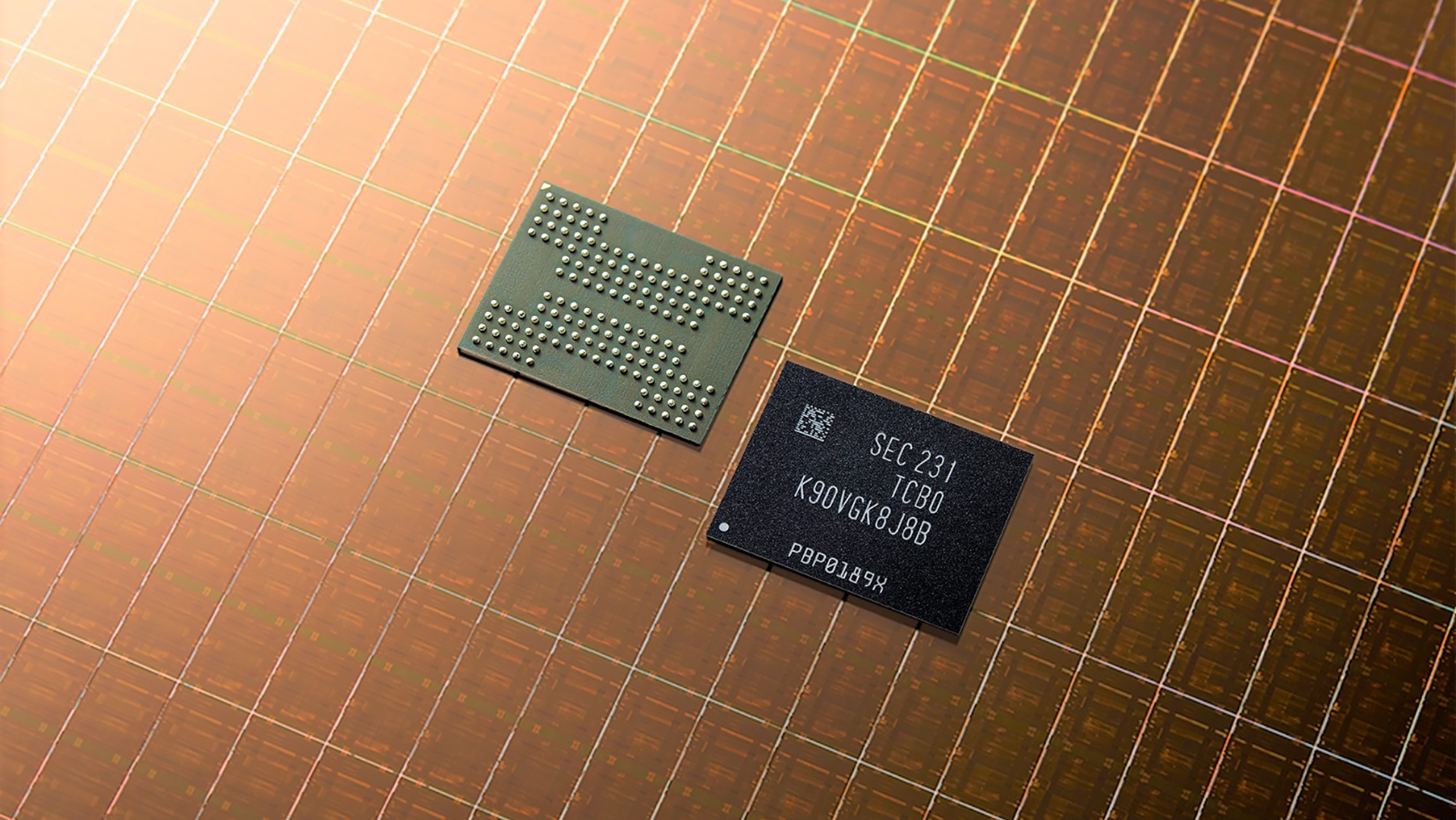
Samsung Electronics is poised to employ double-stack architecture for its 9th Generation 3D-NAND memory when it starts its production next year, according to a DigiTimes report that cites Seoul Economic Daily. The sets Samsung apart from SK Hynix, which uses three stacks of NAND to build its 321-layer 3D NAND devices when they enter mass production in the first half of 2025.
Samsung's 9th Generation V-NAND with over 300-layers is set to hinge on the double-stack technique, which Samsung first embraced in 2020 with its 7th generation 176-layer 3D NAND chips. This method involves production of one 3D NAND stack on a 300 mm wafer and then building another stack on top of the first one. Samsung's 300-layer 3D NAND will increase storage density produced on one wafer and will enable makers to build lower-cost SSDs or make the best SSDs cheaper.
Contrarily, rival SK Hynix has revealed its intent to kick off the production of its 321-layer 3D NAND in 2025 using a triple-stack approach. This procedure, distinct from Samsung's, will involve creating three distinct sets of 3D NAND layers, which will increase the number of steps and usage of raw materials, but is meant to maximize yields as it is easier to produce 3D NAND stacks with fewer layers.
Industry speculations that rely on leaked roadmaps suggest that post their 9th Generation 3D NAND, Samsung might adopt a triple-stack methodology for its 10th generation 430-layer 3D NAND. Some experts told Seoul Economic Daily that surpassing 400 layers in 3D NAND would necessitate usage of three separate stacks of 3D NAND, possibly due to yields concerns. Meanwhile, this will naturally increase usage of raw materials and increase costs per 3D NAND wafer.
Samsung's long-term vision, as presented at the Samsung Tech Day 2022 last October, aspires to reach up to 1,000 layers by 2030.
Get Tom's Hardware's best news and in-depth reviews, straight to your inbox.

Anton Shilov is a contributing writer at Tom’s Hardware. Over the past couple of decades, he has covered everything from CPUs and GPUs to supercomputers and from modern process technologies and latest fab tools to high-tech industry trends.
-
gg83 Can they make an ssd with 300 layers but with slc/mlc? Just make it supper fast with less capacity? Or does it not work that way.Reply -
hotaru251 Reply
maybe?gg83 said:Can they make an ssd with 300 layers but with slc/mlc?
SLC/MLC is just amount of bits in a cell (so their is a limit for each given the physical size you have to work with)
doubt they would though as no profit reason to do so. (slc is very expensive to do)