Samsung Starts Mass Producing 96-Layer 256Gb V-NAND Memory Chips


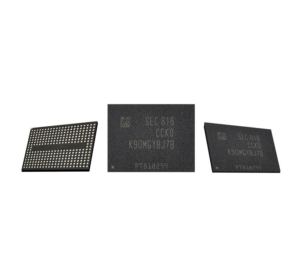
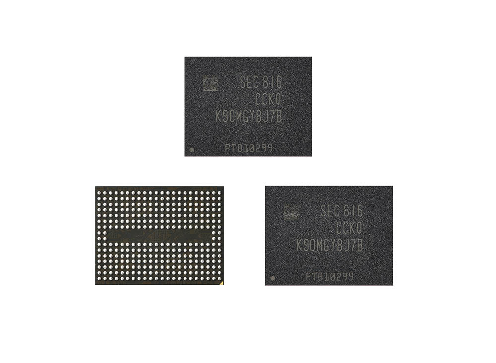
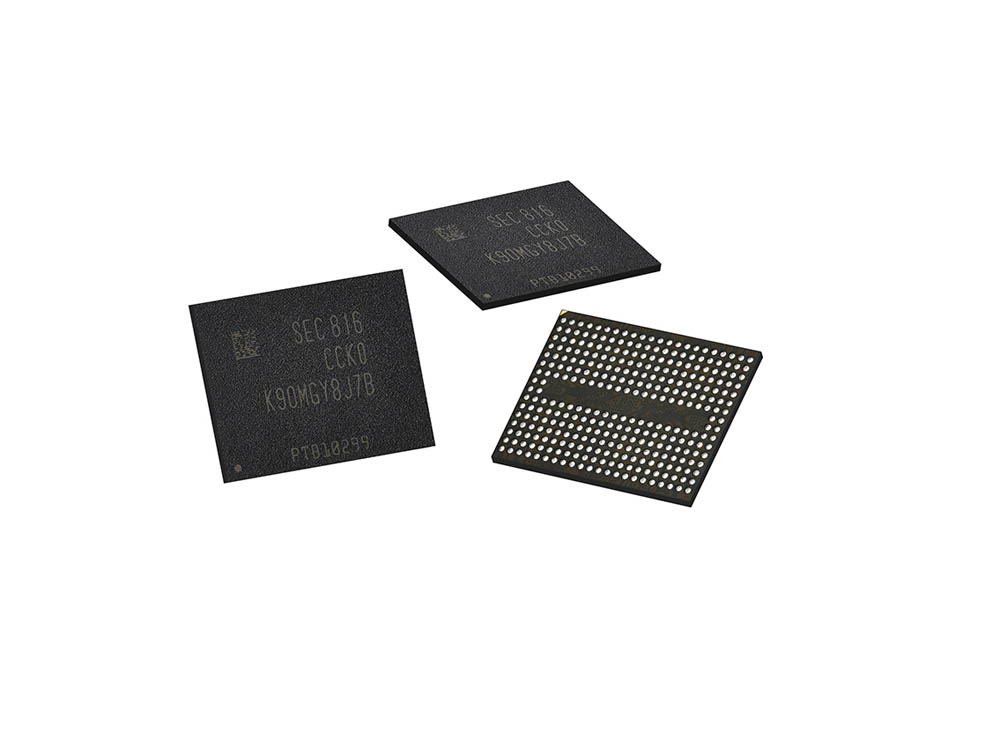
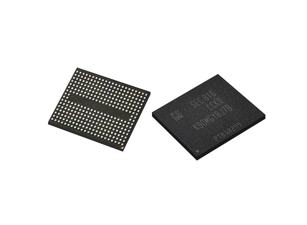
Top NAND manufacturer Samsung announced that it has commenced mass production of its fifth-generation V-NAND memory chips.
There is an increasing need in the market for bigger and faster storage devices, and as the saying goes, “the early bird catches the worm.” Samsung plans to stay ahead of the game with its latest 96-layer 256Gb V-NAND memory chips, which will raise the bar for 3D NAND flash memory.
Samsung's fifth-generation V-NAND memory chips are the first in the industry to exploit the 'Toggle DDR 4.0' interface that acts as a high-speed highway for data to travel up to a speed of 1.4 Gbps between storage and memory. This is a 40% increase over the company's previous 64-layer V-NAND offering. Other performance enhancements include reduction of the data write speed to 500μs, a 30% improvement over its previous generation of V-NAND memory chips, and the response time to read-signals to 50μs. However, the increase in performance is merely the tip of the iceberg. The new 96-layer V-NAND memory chips are also more energy-efficient, boasting an operating voltage of 1.2V as opposed to the previous 64-layer chip's 1.8V.
In order to achieve all the aforementioned improvements, Samsung stacked more than 90 layers of 3D charge trap flash (CTF) cells in the form of a pyramid into the fifth-generation V-NAND memory chip. Each layer features microscopic channel holes that are invisible to the human eye. Nevertheless, the channel holes contain over 85 billion CTF cells capable of storing up to three bits of data each. This method of fabrication is the product of many amazing breakthroughs, including advanced circuit designs and new process technologies. Samsung didn't dwell into specifics, but the company claims that the enhancements in the V-NAND’s atomic layer deposition process has allowed it to increase manufacturing productivity by over 30% and reduce the height of each cell by 20%.
Samsung plans to bring its 96-layer V-NAND memory chips to the markets as soon as possible. The company will initially release them in the 256Gb TLC (three bits per cell) flavor with a larger 1Tb QLC (four bits per cell) chip coming further down the road.
Get Tom's Hardware's best news and in-depth reviews, straight to your inbox.

Zhiye Liu is a news editor, memory reviewer, and SSD tester at Tom’s Hardware. Although he loves everything that’s hardware, he has a soft spot for CPUs, GPUs, and RAM.
-
hotaru251 TBH SSD have been dropping over time. some sales get u a 256gb for 50$~ and 512 at around 80~Reply -
DerekA_C a decent 1tb is now around 180 to 200 I sill want to see that go down to $125 price range where we were with HD about 10 years ago.Reply -
Tanyac 512 for $80.. I wish... More like $250 ($180+ USD) .. 1TB At least $550 ($400+ USD). <sigh>Reply -
hok Honestly the performance is so high now, I wish they will concentrate on Larger storage options for cheaper. I have mostly replaced all my mech drives because they also die within 36 months but I still have my Intel and first samsung SSDs from 6-7 years ago... 2 to 4TB options is what we need.Reply -
Olle P Reply
No, each chip is 512 Gb, which equals 32 GB.21130298 said:So 512GB SSDs will be the new minimum for the consumer?
(Upper and lower case makes a big difference with units!)