SK Hynix Begins Manufacture of 18GB LPDDR5 Memory Packages
SK Hynix begins to make 18GB LPDDR5-6400 memory packages.

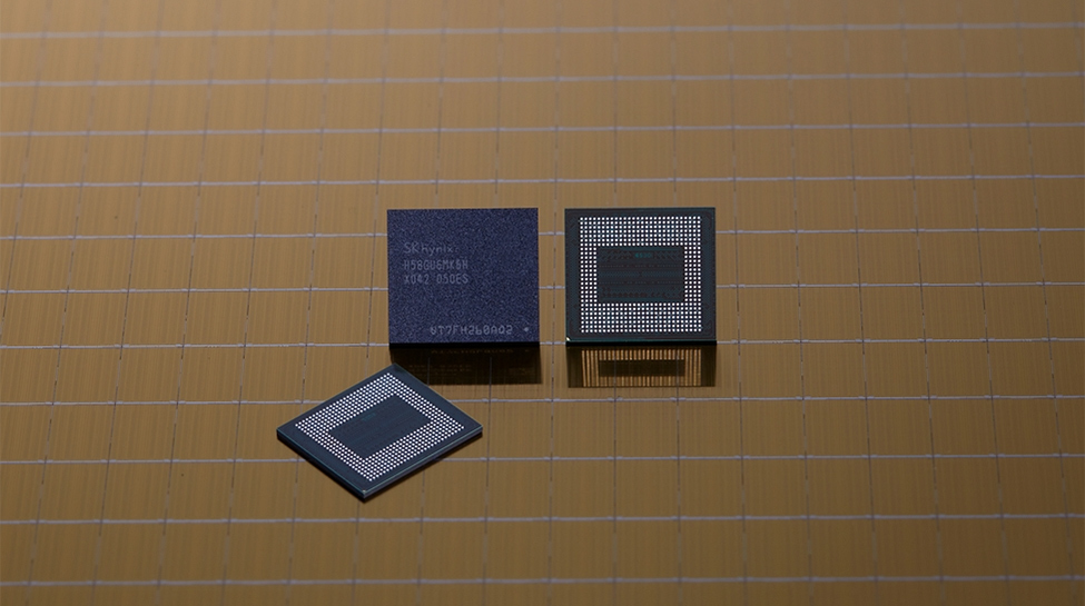
SK Hynix has started volume production of the industry's highest-capacity LPDDR5 memory package. The new device features a 18GB capacity and is designed primarily for high-end smartphones as well as laptops that are powered by system-on-chips which support LPDDR5.
SK Hynix's 18GB LPDDR5 module integrates multiple memory devices and supports a data transfer rate of 6400 Mbps, the highest speed bin supported by the LPDDR5 specification. The new LPDDR5 memory package sees an 11.7% increase in capacity when compared to the previous 16GB modules.
SK Hynix does not disclose which fabrication process it uses to manufacture LPDDR5 memory devices for the 18GB LPDDR5 SDRAM package, but it is highly likely that it uses one of its latest technologies.
One of the first devices to use SK Hynix's 18GB LPDDR5-6400 memory module is the Asus ROG 3 gaming smartphone. Eventually, the same package can be integrated into laptops or tablets with 18GB or even 36GB of memory.
Get Tom's Hardware's best news and in-depth reviews, straight to your inbox.

Anton Shilov is a contributing writer at Tom’s Hardware. Over the past couple of decades, he has covered everything from CPUs and GPUs to supercomputers and from modern process technologies and latest fab tools to high-tech industry trends.
-
MarsISwaiting DDR 2 DDR 3 DDR 4 DDR 5 .. why arent we going TDR or QDR ? been using DDR technology long time alreadyReply -
DSzymborski ReplyMarsISwaiting said:DDR 2 DDR 3 DDR 4 DDR 5 .. why arent we going TDR or QDR ? been using DDR technology long time already
Triple data rate would be quite awkward. DDR and QDR configure logically around the rising and falling of the clock signal; QDR uses separate data buses for read and write. At last check, QDR was absurdly expensive, making it unsuitable for consumer applications. -
InvalidError Reply
The only thing QDR does is reduce the amount of power needed to drive the bus clock at the expense of extra circuitry in the GDDR5+ chips to internally generate the extra edges for the QDR IOs.MarsISwaiting said:DDR 2 DDR 3 DDR 4 DDR 5 .. why arent we going TDR or QDR ? been using DDR technology long time already
No, QDR only means nothing more than the data rate is 4X the clock frequency. Even GDDR6X with its new PAM4 signaling still shares IO pins between reads and writes. What "got split" with GDDR6 is that the chips are internally structured as two independent 16bits-wide banks, so you can configure them as either 1x32bits or 2x16bits.DSzymborski said:QDR uses separate data buses for read and write. -
DSzymborski https://www.latticesemi.com/products/designsoftwareandip/intellectualproperty/referencedesigns/referencedesign04/qdr-sram-memorycontroller#_F8CEC1864D734E5B9511AC7C69DDF420Reply
Hmm, what's the source of my confusion then? I'm unsure now. -
InvalidError Reply
You equated QDR to having separate DDR R/W ports. Those two things are completely unrelated, GDDR5/5X/6/6X all have single QDR data ports.DSzymborski said:Hmm, what's the source of my confusion then? I'm unsure now.
The chip you linked is an SRAM that takes commands and operates at QDR internally so it can then split its internal bandwidth between its separate DDR read and write ports. Quite different application from GDDR5+ which has DDR command and single-port QDR data.
Also, the main reason your SRAM chip is "absurdly expensive" isn't QDR, it is simply the fact that it is an SRAM chip and those are inherently far more expensive to make per bit due to much lower density. Also doesn't help that it is a relatively low bandwidth (192MHz max clock) niche product intended to supplement FPGA SRAM, which makes it a (very) low volume part and further drives cost up. -
InvalidError Reply
Nothing special about it, DDR4 DIMMs are available in 18GB and 36GB sizes due to ECC.thisisaname said:18GB is a rather odd amount of memory.
With DDR5, ECC becomes standard across the board so DRAM manufacturers can use smaller DRAM cells without worrying too much about increased error rates. -
hotaru.hino Reply
Looking around for ECC DDR4 RAM modules, they advertise their usable memory size, not total memory size.InvalidError said:Nothing special about it, DDR4 DIMMs are available in 18GB and 36GB sizes due to ECC.
Looks like someone in marketing convinced the higher ups to drink the numbers koolaid. -
InvalidError Reply
Not really. This announcement is about DRAM packages and bare chips have pretty much always been marketed based on raw specs. The only difference here is that prior to DDR5, ECC was optional and was implemented by including the extra DRAM package(s) for ECC bits.hotaru.hino said:Looks like someone in marketing convinced the higher ups to drink the numbers koolaid.
Now that ECC is becoming standard and DDR5 DIMMs have split the slot into two independent sub-channels, it makes more sense to build the extra bits directly into the individual DRAM chips than have to add an oddball 4-bits wide DRAM for ECC to each half of a 36+36 bus setup.