SK Hynix Envisions 600-Layer 3D NAND & EUV-Based DRAM
SK Hynix demonstrates its conceptual technology roadmap.

On Monday executives at SK Hynix gave a keynote speech to the IEEE International Reliability Physics Symposium (IRPS) where they shared their vision about the company's mid-term and long-term technological goals. SK Hynix believes it can continue increasing capacity of its 3D NAND chips by increasing the number of layers to over 600. Furthermore, the company is confident that it can scale DRAM technologies below 10nm with the help of extreme ultraviolet (EUV) lithography. Ultimately, SK Hynix wants to converge memory and logic into one device to address emerging workloads.
"We are improving materials and design structures for technical evolution in each field of DRAM and NAND, and solving the reliability problems step by step," said Seok-Hee Lee, CEO of SK Hynix. "If the platform is innovated successfully based on this, it is possible to achieve the DRAM process below 10nm and stack over 600 layers of NAND in the future."
The Future of 3D NAND: 600-Layers and Counting
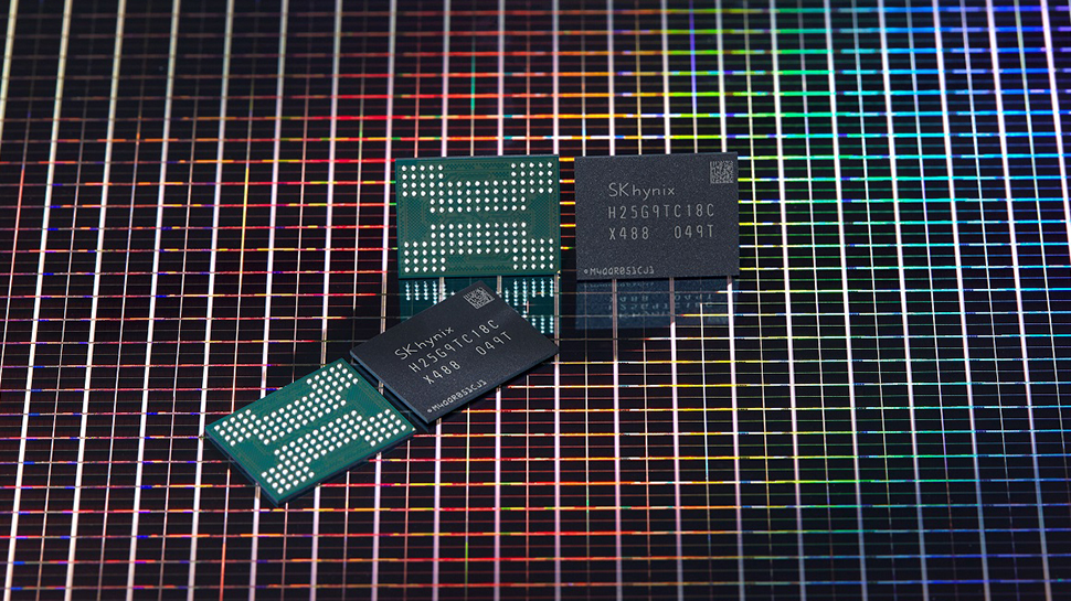
3D NAND has proven to be a very efficient architecture both in terms of performance and scalability, so SK Hynix will continue using it for years to come. Back in December, 2020, SK Hynix introduced its 176-layer '4D' 3D NAND memory with a 1.60 Gbps interface. The company has already started sampling 512Gb 176-layer chips with makers of SSD controllers, so expect drives based on the new type of 3D NAND memory sometimes in 2022.
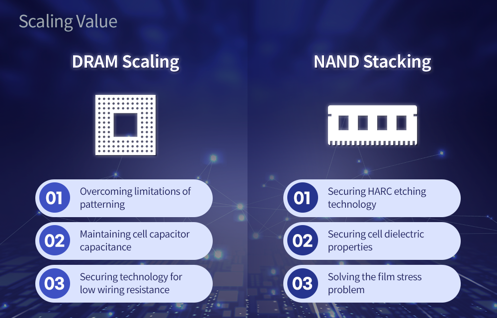
Just a few years ago the company believed that it could scale 3D NAND to ~500 layers, but now it is confident that it can scale it even beyond 600 layers in the long-term future. By increasing the number of layers, SK Hynix (and other producers of 3D NAND) will have to keep making layers thinner, NAND cells smaller and introduce new dielectric materials to maintain uniform electric charges therefore preserving reliability. The company is already among the leaders in atomic layer deposition, so one of its next goals is to implement high aspect ratio (A/R) contact (HARC) etching technology. Also, for 600+ layers it will probably have to learn how to string stack more than one wafers.
SK Hynix did not even imply when the industry should expect 3D NAND devices with over 600 layers and what capacities will such incredible number of layers bring. With its 176-layer technology SK Hynix is looking at 1Tb products, so with 600 layers per-device capacities will get even more impressive.
The Future of DRAM: Below 10 nm with EUV
Just like Samsung Semiconductor and unlike Micron Technology, SK Hynix believes that adoption of EUV lithography is the most straightforward way to keep increasing performance of DRAM while also boosting capacity of memory chips and keeping their power consumption in check. With DDR5, the company will have to introduce memory devices with a capacity of over 16Gb and data transfer rates of up to 6400 GT/s (initially) that will be stacked together to build high-capacity DRAM chips.
Since future memory products will have to bring together high performance, high capacity, and limited power consumption, advanced manufacturing technologies will get even more important. To successfully implement EUV, SK Hynix is developing new materials and photoresists for stable EUV patterning and defect management. In addition, the company is looking at innovating the cell structure while maintaining its capacitance by using thinner dielectrics made of materials with high dielectric constant.
Get Tom's Hardware's best news and in-depth reviews, straight to your inbox.
It is noteworthy that SK Hynix is now also looking at ways to reduce resistance "of the metal for interconnect", which is an indicator that the sizes of DRAM transistors have gotten so small that their contacts are about to become a bottleneck. With EUV, transistors will shrink their sizes, gain performance, and reduce their power, so contact resistance will indeed become a bottleneck somewhere at 10nm or below. Producers of logic solved this issue in different ways: Intel decided to use cobalt instead of tungsten, whereas TSMC and Samsung Foundry switched to selective tungsten deposition process. SK Hynix did not elaborate about its way to fight contact resistance, but only said it was seeking "next-generation electrode and insulating materials and introducing new processes." It remains to be seen what DRAM makers will use to lower contact resistance, but it is evident that memory makers have essentially the same issues as their logic peers.
Converging Processing and Memory
In addition to making DRAM faster and boosting its capacity, SK Hynix is looking forward to converging memory and processing. Nowadays leading-edge processors for supercomputers use high-bandwidth memory (HBM) that is connected to them using an interposer. SK Hynix calls this concept PNM (Processing Near Memory). SK Hynix asserts that the next step is PIM (Processing In Memory) with the processor and the memory existing within a single package, whereas ultimately the company is looking at CIM (Computing in Memory), where the CPU and the memory is integrated into a single die.
To a large degree, SK Hynix's CIM concept resembles Samsung's PIM (Processing in Memory) concept introduced this past February and set to become an industrial standard defined by JEDEC. Samsung's HBM-PIM embeds 32 FP16-capable programmable computing units (PCUs) that run at 300 MHz into a 4Gb memory die. The PCUs can be controlled using conventional memory commands and execute some basic computations. Samsung claims that its HBM-PIM memory is already under trials in AI accelerators with leading AI solutions providers and indeed the technology makes a lot of sense for AI and other workloads that do not require high precision, but benefit from the number of simplistic cores that can be made using DRAM fabrication processes.
At this point it is unclear whether SK Hynix's CIM will be implemented in accordance with the upcoming JEDEC standard proposed by Samsung, or SK Hynix will go with a proprietary technology. But at least the largest makers of DRAM in the world have similar vision about converged memory and logic devices.
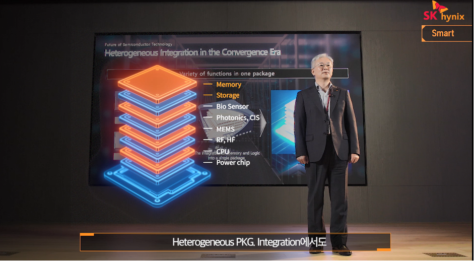
Converging logic and memory makes a lot of sense for niche applications. Meanwhile, there are more common applications that that can benefit from tighter integration of memory, storage, and processing. To that end, SK Hynix is developing heterogeneous computing interconnect technology for tightly integrated packages containing processing IP, DRAM, NAND, micro-electro-mechanical systems (MEMS), radio frequency identification (RFID), and various sensors. Again, the company did not provide many details here.

Anton Shilov is a contributing writer at Tom’s Hardware. Over the past couple of decades, he has covered everything from CPUs and GPUs to supercomputers and from modern process technologies and latest fab tools to high-tech industry trends.


