TSMC Confirms Plans to Start 3nm Production Shortly
TSMC’s 3nm era set to begin in the coming weeks
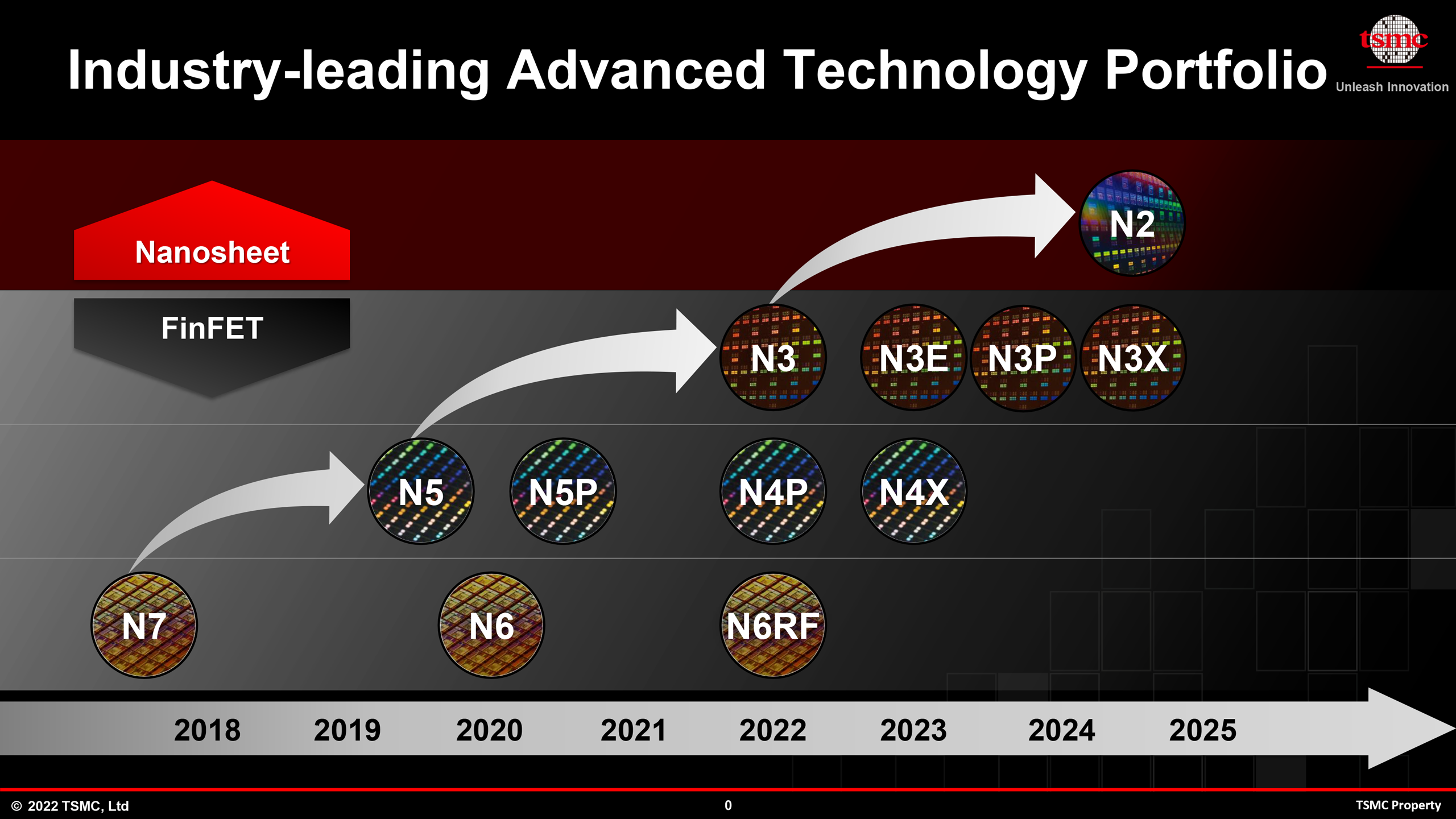
TSMC (Taiwan Semiconductor Manufacturing Co.) is set to start production using its N3 (3nm-class) fabrication process shortly, the company said at an event on Tuesday. Formally, the company does not disclose customers who plan to use its N3 manufacturing technology first, but unofficial sources indicate that Apple will be TSMC's alpha customer for the production node.
TSMC intends to kick off high volume manufacturing of chips on its N3 fabrication technology 'soon,' according to C.C. Wei, chief executive of the world's largest contract maker of semiconductors, reports Nikkei. Previously, unofficial sources indicated that TSMC intended to start producing chips on its N3 production node in September, but this is the first time the company has confirmed that it has not started to make products on its most advanced node yet and that it plans to start high-volume manufacturing (HVM) of 3nm chips 'shortly.'
When compared to TSMC's N5 fabrication process that entered HVM in 2020, the foundry's first generation N3 fabrication process promises to deliver a 10% to 15% performance improvement (at the same power and complexity), reduce power consumption by 25% – 30% (at the same speed and transistor count), and increase logic density by around 1.6 times.
| Row 0 - Cell 0 | N3E vs N5 | N3 vs N5 |
| Speed Improvement @ Same Power | +18% | +10% ~ 15% |
| Power Reduction @ Same Speed | -34% | -25% ~ -30% |
| Logic Density | 1.7x | 1.6x |
| HVM Start | Q2/Q3 2023 | H2 2022 |
Eventually, TSMC plans to add more nodes to the N3 family. N3E will deliver an improved process window, N3P targets enhanced performance, N3S will offer increased transistor density, and N3X will have further performance optimizations for applications like CPUs. As you might expect with the slowing down of Moore's Law, the 3nm family of nodes will be used for many years to come.
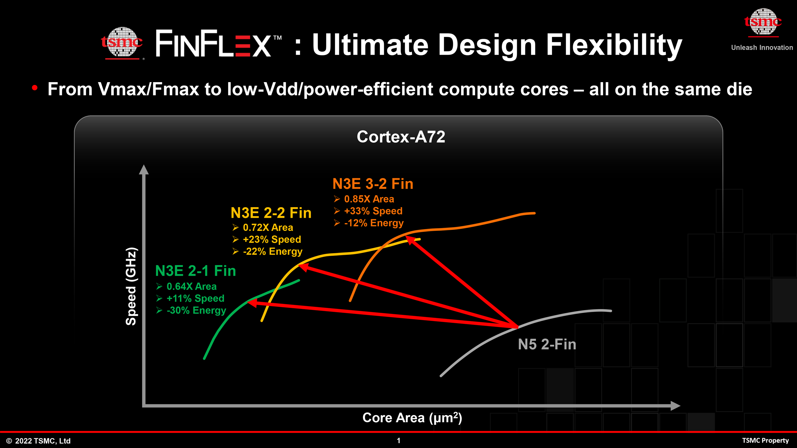
One of the key features of N3 is TSMC's FinFlex technology that greatly enhanced design flexibility for fabless chip developers. The tech allows designers to mix and match different kinds of standard cells within one block to accurately optimize performance, power consumption, and area, which will be especially advantageous for complex devices like CPU or GPU cores that have to offer both high transistor density and high clocks. As a result, companies who build complex system-on-chips — such as Apple, AMD, Intel, MediaTek, and Nvidia — will benefit from FinFlex.
Apple, which is TSMC's largest customer, is expected to be the first company to adopt the foundry's N3 technology, though it is unclear what exactly the company plans to produce using this node. Later on, the technology will be used by Intel as well as other clients of TSMC, including AMD, Nvidia, MediaTek, and Qualcomm.
Get Tom's Hardware's best news and in-depth reviews, straight to your inbox.

Anton Shilov is a contributing writer at Tom’s Hardware. Over the past couple of decades, he has covered everything from CPUs and GPUs to supercomputers and from modern process technologies and latest fab tools to high-tech industry trends.

