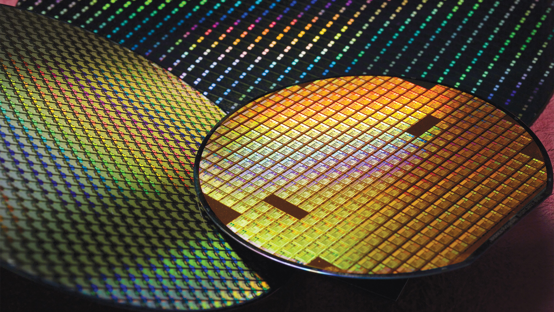
TSMC Forms Task Force to Accelerate 2nm Chip Production
TSMC seemingly assembles One Team to work on 2nm fabrication process.

TSMC has formed an internal 'One Team' task force dedicated to timely development, trial production, and mass production of its N2 (2nm-class) process technology, according to reports from CNA and TorrentBusiness (via@DanNystedt). The 'One Team' approach suggests a unified and concerted effort, bringing together expertise and resources to streamline the development and implementation of the 2nm process.
Forming a special task force is somewhat out of character, as TSMC typically launches pilot and then mass production on its latest fabrication technologies at one fab. This time around, according to reports, things will be different. TSMC has plans to commence simultaneous pilot production on its N2 process at two fabs at its Hsinchu site: one in Baochan and another in Kaohsiung. The company intends to start pilot production at both locations in 2024 and initiate volume production in 2025.
TSMC is developing N2 fabrication technology at its special R&D center near Hsinchu. Hence, the fabs are close to the research and development facility, making it easier for fab engineers to communicate with teams that developed the manufacturing process. Meanwhile, TSMC is reportedly transferring 300 employees from its Fab 15A and 400 employees from its Fab 15B near Taichung to its fabs to 'support the 2nm projects.'
TSMC confirmed the establishment of the 'N2 One Team' task force but refrained from disclosing detailed information about its structure and specific projects, according to TorrentBusiness. An intriguing detail here is that the website mentioned projects instead of project when discussing TSMC's N2. The world's No.1 foundry is working on multiple 2nm-class projects, including N2 that introduces gate-all-around nanosheet transistors for early 2026, N2P that add backside power delivery in early 2027, and N2X with extended performance due later this decade. Meanwhile, based on the report, N2 is coming to the two fabs at the Hsinchu site.
Intensified competition in the field of leading-edge process technologies is perhaps one of the key reasons why it is making notable shifts in its strategy and resources. On the one hand, Intel Foundry Services is set to offer its 2nm and 1.8nm-class process technologies to its clients about two years ahead of TSMC. In contrast, Samsung Foundry is getting more competitive in general, which is why it may win some production contracts on proven nodes.
Another potential reason for TSMC assembling a special task force to expedite its 2nm endeavors is the heightened complexity of modern nodes. The cadence for introducing new nodes has expanded from two years, as seen with N7 and N5, to approximately three years with N3. Mass production on TSMC's N2 node is anticipated to commence in late 2025 or early 2026, marking roughly three years since the initiation of high-volume manufacturing for N3.
Obviously, TSMC wants to streamline its N2 development and implementation as much as possible, so forming a special task force makes sense. Yet, launching pilot production and the HVM at two fabs (albeit adjacent) is also a significant challenge.
Get Tom's Hardware's best news and in-depth reviews, straight to your inbox.

Anton Shilov is a contributing writer at Tom’s Hardware. Over the past couple of decades, he has covered everything from CPUs and GPUs to supercomputers and from modern process technologies and latest fab tools to high-tech industry trends.
-
pointa2b Perhaps with the increased manufacturing costs and difficulty of making it work, going forward this will become a regular thing.Reply -
Eximo ReplyNeoMorpheus said:Please forgive my dumb question, but whats next after 1nm or 0.x nm?
Next unit down. Angstroms.
Intel 20A (2nm) class is the first to be named such, and they already have 18A in the works.
Though these numbers already have little to do with actual silicon features. Just how accurate they can lay things out, not necessarily the size of measurable features.
Density increases are going to come more from switching to GAA in place of FinFET and doing power delivery on the back.
As to how they plan to reach sub 1nm, not a clue, that is probably not targeted until the 2030s. Not to mention that progress has been slowing down as they reach the limits of what physics allows. (Gets said a lot, but a silicon atom is only about 1.5 angstrom across, so not too far off) -
dehjomz I wonder if competition from Intel 18A has anything to do with this aggressive move by TSMC. Next will we hear that TSMC is cutting wafer pricing ?Reply -
Eximo Intel typically reserves their smallest node for CPU logic, so they aren't competing in the open market with anyone but AMD and to a lesser extent Apple.Reply
TSMC is still ahead of Intel in terms of efficiency even with AMDs current x86 parts. But Apple likes to pay for exclusivity on their best node so M2 is a step above that.
Intel and TSMC are building additional fabs. TSMC has a lot of work to do to establish supply lines and workforce outside of Taiwan. Intel has an advantage there, in that their US based fabs and other fabs/diffusion/design endeavors are already pretty well globalized.
Intel Foundry may begin offering its services in the same way that TSMC does, but that isn't for a while longer. It will be very interesting to see how this all plays out. -
usertests Reply
Since the names have little meaning, focus on the technologies.NeoMorpheus said:Please forgive my dumb question, but whats next after 1nm or 0.x nm?
GAAFET starting at N2 and some further nodes. Complementary FETs later. Maybe vertical nanowire FETs (SRAM only?). Carbon nanotube FETs?
At the same time, 3D packaging technologies will gain more importance, possibly more than the transistor technologies used. -
Geef I'm imagining the boss in Taiwan saying "OK task force, you normally work 6 days a week 20 hour days. Now that we need to accelerate production we are changing to 7 days a week and 21 hour days."Reply
"Oh, and call off Christmas!" -
TerryLaze Reply
You made me google if people celebrate christmas in taiwan....Geef said:I'm imagining the boss in Taiwan saying "OK task force, you normally work 6 days a week 20 hour days. Now that we need to accelerate production we are changing to 7 days a week and 21 hour days."
"Oh, and call off Christmas!"
( only about 5% are christian) -
Co BIY There is a good chance that the global market for advanced microprocessors is going to grow so fast that TSMC and Intel can both increase production as much as reasonably possible without creating an oversupply.Reply -
ToBeGood Reply
1nm 0.x nm is just a marketing slogan,NeoMorpheus said:Please forgive my dumb question, but whats next after 1nm or 0.x nm?
Just give you a food for through silicon atom is 0.2 nm so you think a transistor can be anywhere 9 atoms wide (it just very difficult.
