UCLA Finds Layout Design Important In Transistor Performance
Get Tom's Hardware's best news and in-depth reviews, straight to your inbox.
You are now subscribed
Your newsletter sign-up was successful
Los Angeles (CA) - A team of UCLA researchers has been able to increase the performance of transistors by at least 5% without changing anything in the manufacturing process. Instead, they looked only at the up-front design used to create the circuit's shape. The research produced wires that were 30% shorter than standard models, as are used for logic gates, interconnects and nodes. They've found that by only optimizing the layout during the computer design stage, additional performance and speed is achievable without any other considerations.
While this might seem like a no-brainer, it all comes down to taking the time to do the math. According to Jason Cong, a UCLA professor and chair of computer science, "It's fairly easy to model this problem mathematically. You can think of nodes as points on a graph, and you can think of the interconnects as hyper-edges that connect more than two noes. We can use mathematics to determine how the placement problem should be solved. We use a mathematical technique called multiscale methods, in which we group nodes together until we get a mathematical problem that is small enough to solve". Eric Radke, a UCLA mathematics graduate student, said, "We have found there is a huge amount of room for improvement in the physical design of the chip itself, including where nodes are placed."
Potential hurdle
There is a potential hurdle to such a technique. When moving from 130nm to 90nm, CPU designers faced some difficult challenges they had not previously encountered. There was a significant jump in compilation software required for modeling 90nm circuits. Whereas the software used at 130nm was able to draw straight lines by simply drawing straight lines, this process no longer worked at 90nm. As feature sizes shrank relative to the large wavelength of laser light used in manufacturing, something new was needed.
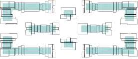
The designers began including all kinds of nearby lines, squares and rectangles, shapes which do not accurately describe the true path, but shapes which focus the laser light correctly so it impacts where they need it to. Working out exactly how to do this was one of the big delay factors in migrating to that process generation.
Today, rather than having a simple list of lines in a database, each of which describes its part of a 3D circuit in a specific manufacturing layer, there now exists a complex database of related shapes which, when applied mathematically to the real-world characteristics of current laser technology, draws the circuit lines where they should be, as the author's design originally intended.
The end result of OPC is a series of rectangles, boxes, lines and squares which like the following image, just to make a series of very small straight lines:
Chan, Cong and their graduate students won an award in 2005 for their work at the International Symposium of Physical Design (ISPD). Their placement software, developed together with their former students Kenton Sze and Min Xie, produced the best wire-length results in a 2006 Circuit Placement Contest, also organized by ISPD. Their research is funded by the National Science Foundation and the Semiconductor Research Corporation, the world's leading university research consortium for semiconductors (and related technology).
Get Tom's Hardware's best news and in-depth reviews, straight to your inbox.
Author's opinion
I would be very surprised to learn that major production manufacturing entities like Intel, Samsung, AMD, etc., aren't already taking such transistor design considerations into account. I would think that at that point, everything would be about as highly optimized as it can reasonably be for a production manufacturing process. However, it might be that it hasn't been needed yet. An increase of 5% is nice, but if it would require a revamp of their entire compilation algorithms to get there, it might not be worth it.

