Wafer Scale Quantum Chip Prototype to Accelerate Qubit Counts
It is a quantum renaissance for fabrication industries.

Get Tom's Hardware's best news and in-depth reviews, straight to your inbox.
You are now subscribed
Your newsletter sign-up was successful
French research institutions CEA and C12 Quantum Electronics have announced a novel quantum computer design. One that can only describe as a waferscale engine... for quantum. In an approach to CMOS manufacturing techniques and backed by the CEA's $5 billion annual funding, the companies aim to manufacture carbon nanotube-based qubits at scale - a 200 mm (7.9 inches) wafer at a time. As a result, transistor density now sees itself as a parallel to quantum density.
There have been some other quantum computing designs that aim to approximate themselves with transistor manufacturing in one way or another. The idea is that the more compatible qubit manufacturing is to that of existing silicon-aimed processes (such as those of TSMC's 4N or Intel 7), the more efficiently manufactured - and scaled - they can be.
But none of the presented designs were for an entire 200 mm wafer scale. It's telling that in the $599.9 billion-dollar-worth semiconductor market, only Cerebras has deemed to build a waferscale chip. The difficulties in such a design are tremendous, yet C12 expects to have a working, final waferscale prototype by the end of the decade.
Article continues below"Quantum technology offers great promise for the next computing generation but still faces significant developmental challenges for fabricating qubit chips," said Sébastien Dauvé, CEO of the CEA-Leti lab. "Combining well-established CMOS technologies with C12's original approach using carbon nanotubes could accelerate progress toward commercializing quantum computing and manufacturing those chips at scale."
C12 is confident: its technologies allow for ease of fabrication (relative to the more exotic approaches to quantum computing) that approaches that of a semiconductor device and would allow for a "scalable and ultra-coherent platform for quantum computing." Pierre Desjardins, CEO and co-founder of C12, said the ultimate aim is to "transfer an academic fab process to an industrial-grade semiconductor fab process."
The company says it can manufacture thousands of qubits per hour - and ultimately achieve densities in the order of the "hundreds of thousands" of qubits per wafer-sized quantum computing chip. The company's initial design goal was to focus on delivering a million-qubit quantum computer. Perhaps it ultimately doesn't need to be delivered within a single wafer.
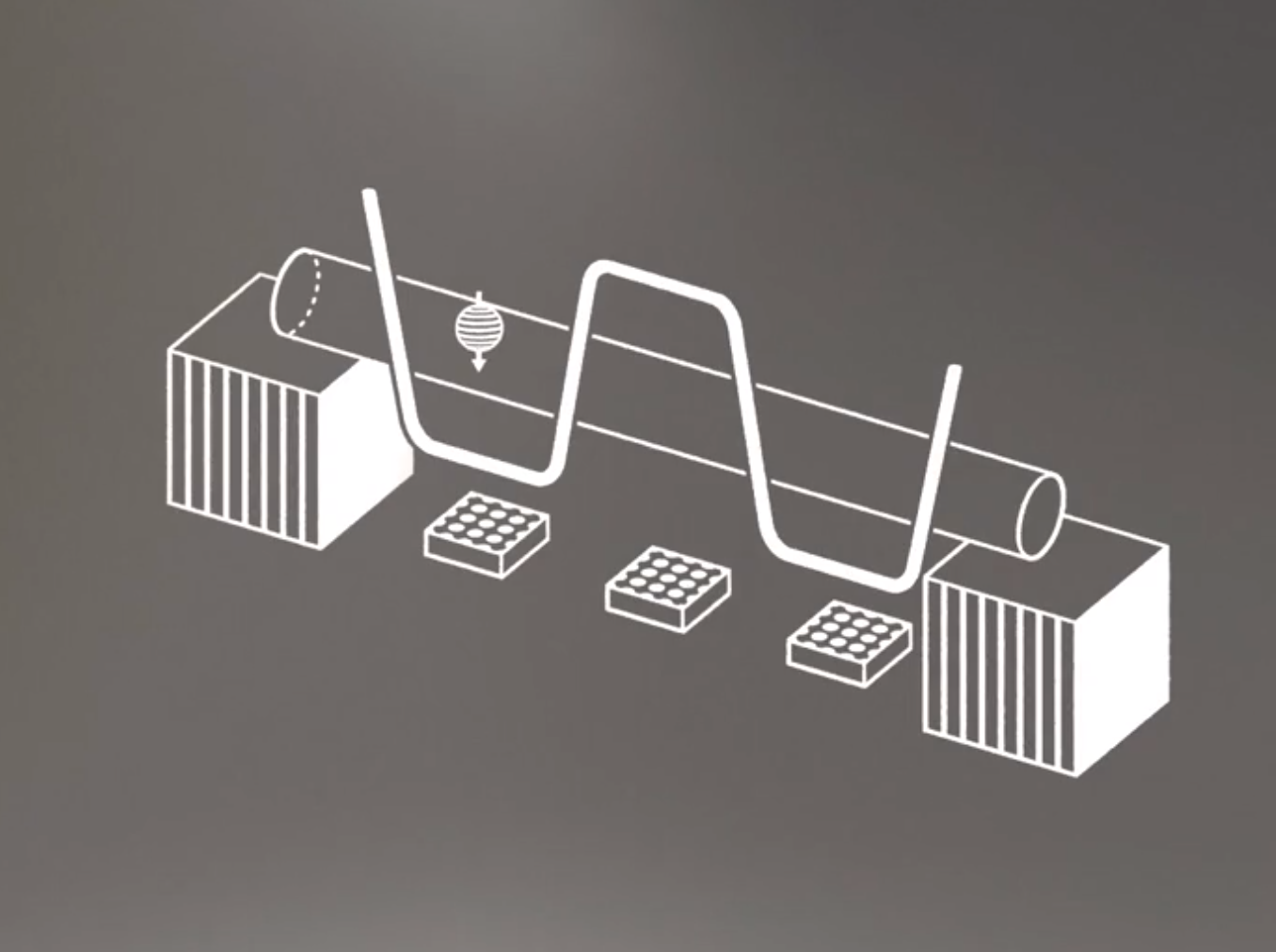
C12's qubit design starts with the growth of ultrapure carbon nanotubes, which the company does within its facilities to guarantee their purity level. Then, via chemical vapor deposition, C12 isotopes of carbon are meticulously placed - atom by atom - to form the nanotube structure.
Get Tom's Hardware's best news and in-depth reviews, straight to your inbox.
It is inescapable because the presence of any other isotope (or atomic particle) in the nanotubes would lead them to interact. That would, in turn, increase the dreaded "spin noise" - one of the primary sources of disturbances within quantum machinery that can lead qubits to collapse entirely, originating errors in calculations or interrupting workloads. So before they used nanotubes anywhere, they screened them for impurities non-invasive. Only those with a 99% purity (meaning they contain 99% C12 carbon isotopes) make it to the next step.
The carbon tubes are then meticulously placed on IC chips produced in massive scales already by the semiconductor manufacturing industry. The carbon nanotubes lay suspended above an array of gate electrodes, ensuring optimized environmental isolation for "drastically reducing decoherence due to charge and mechanical noise." A novel, microwave-based regulator, allows for the system's qubits to be coupled at will between one another. It simultaneously improves performance while reducing the environmental interference of changes to qubits' states.
Considering the already copious inspiration from the semiconductor industry, the thought that two of these wafer-scale computing chips could then scale through a networking solution (perhaps photonic based) sounds like the subsequent path of least resistance.
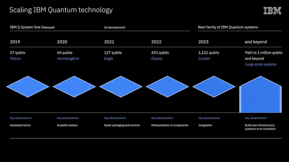
We must remember that the announcement comes before a working prototype - but after the actual hardware test runs already. Today, IBM's Eagle quantum computer counts 127 qubits, and IBM has previously said it would reach a million-qubit density by 2030. With CEA and C12's million-qubit prototype, there's another real contender for a pole position in that particular pursuit. But many metrics are responsible for a quantum computer system's performance, and other companies (such as incomparably wealthy Microsoft) are definitely in the race.

Francisco Pires is a freelance news writer for Tom's Hardware with a soft side for quantum computing.
-
husker In the first 42 years of quantum computing research we go from 0 to 127 qbits. In the next three years we go from 127 to 1,000,000. Sounds about right.Reply


