
The launch of the Nvidia RTX 40-series and Ada Lovelace GPUs has been greeted with a range of emotions. Excitement from some, disbelief from others, and outright scorn from many. In building a GPU that promises to outperform the best graphics cards, Nvidia has gone big — big and expensive. AMD, on the other hand, is using a more cost-effective technology that could make its upcoming RDNA cards more appealing, more affordable choice.
While we're not privy to Nvidia's Bill of Materials (BOM), the high price of Nvidia's GPUs is largely due to the company's refusal to embrace "Moore's Law 2.0" and look to things like chiplets. AMD started beating Intel on CPUs when it switched to chiplets, especially on cost, and now they're about to do the same for GPUs. Putting the analog memory interfaces on an older process with RDNA 3 is a brilliant approach, since analog scales very poorly with newer process nodes. The same goes for cache.
Looking at the AD102 die shots Nvidia has posted so far, we know the die size is 608mm^2. That's only slightly smaller than GA102 at 628mm^2, but now Nvidia is on a cutting edge TSMC 4N process node instead of Samsung 8N. Pricing on the wafers definitely shot up, and we had multiple stories in the past year about TSMC raising prices. That's all coming to bear.
The AD102 die pictured below — which is a rendering but it's the best we've got — shows some clear details of how and why Nvidia's latest tour de force costs more than the previous generation chips. Flip through the gallery for annotated versions of the image.


The twelve Graphics Processing Clusters (GPCs) are easily distinguishable from the rest of the chip, and each of those has 12 Streaming Multiprocessors (SMs). All of the GPCs and SMs together take up about 45% of the total die area. Where does the rest go?
The twelve 32-bit GDDR6X memory controllers use up most of the outside edge of the die, with the PCIe x16 connector using about a third of the bottom edge. The memory controllers and related circuitry take up a hefty 17% of the die area, give or take. But that's not the only part of the memory subsystem, as Nvidia has a much larger L2 cache than on previous designs.
You can see the six 16MB chunks of L3 in the center section of the die, with some related routing and other circuitry (ROPs?) around it. The L2 cache blocks are at least 15% of the total die area, while the entire center portion of the die (L2 plus other logic) takes up 25% of the total. The remainder of the die at the bottom is dedicated to things like the dual NVENC encoders, the PCIe interface and physical display interfaces. It's about 7% of the total, and then there are a few other miscellaneous bits scattered around that take up the last ~6% of the die.

The point of discussing those die areas is to help put things in perspective. Nvidia, with its monolithic approach on the AD102 chip, has dedicated roughly 33% of the total die area just to memory interfaces and L2 cache. AMD's MCD (Memory Chiplet Die) approach used with its Radeon RX 7000-series and RDNA 3 GPUs will apparently move nearly all of that off the main chiplet, and it will reportedly use TSMC N6 instead of TSMC N5, reducing price and improving yields at the same time.
TSMC doesn't reveal its contract negotiations with large partners like Apple, AMD, Intel, or Nvidia. However, there are reports that TSMC N5 (and thus 4N, which is more or less just "refined" N5) costs at least twice as much as TSMC N7/N6. With a 608mm^2 die size for AD102, Nvidia can only get around 90 full dies per wafer — and for reference, that's only about two more chips per wafer than GA102.
If TSMC 4N costs more than twice as much per wafer as Samsung 8N, that means AD102 costs more than twice as much per chip as the previous generation GA102 and the RTX 3090. Gordon Mah Ung of PC World asked Nvidia CEO Jensen Huang during a Q&A session about pricing. I'll go ahead and quote it directly to put things in context.
Gordon: [RTX] 4000 is finally here, which for you I'm sure feels like a huge launch. The reaction universally I'm seeing out there is, "Oh, my God. It costs so much money." Is there anything you would like to say to the community regarding pricing on the new generational parts? As well as, can they expect to see better pricing at some point and basically address all the loud screams that I'm seeing everywhere?"
Jensen: "First of all, a 12 inch wafer is a lot more expensive today than it was yesterday. And it's not a little bit more expensive, it is a ton more expensive. Moore's law is dead. And the ability for Moore's law to deliver the same performance, half the cost every year and a half is over. It's completely over. And so the idea that the chip is going to go down in cost over time, unfortunately is a story of the past." (Emphasis added.)
Of course, there's a lot more to building a graphics card than just the GPU. Memory, PCB, VRMs, PMICs, capacitors, and all sorts of other bits are involved. Prices on many of those have increased over the past two years as well. Nvidia also has to put a lot of effort into the research and development of GPUs and related technologies. And the final design has to take all of that into account and then ultimately turn into a successful product.
So how much does a new part need to cost in order to make for a profitable product? That's more difficult to say.

One more interesting thing about the RTX 40-series announcement is that Nvidia has revealed three different graphics card models, and each one uses a different GPU. Again, that sort of approach has to increase costs, and it means Nvidia also needs to figure out how to best allocate its wafer orders. The AD102 chip in the RTX 4090 is the new halo part with a large die and all the trimmings. AD103 cuts down the memory interface and the core counts, and then AD104 cuts them down even further.
Nvidia hasn't released die shots or renderings of AD103 and AD104 just yet, but we do have the full specs. They're quite a bit smaller, and much of that comes from reducing core counts, memory interfaces, and L2 cache size. The 4080 models will naturally be higher volume products than the 4090, though it's worth pointing out that the 4090 potentially has 70% more compute, 50% more memory bandwidth and capacity, and uses 41% more power, all while "only" costing 33% more. In other words, RTX 4080 16GB pricing is proportionately worse than the RTX 4090.
We can do the same for the RTX 4080 12GB. The 4080 16GB offers 21% more compute, 33% more memory capacity, 42% more memory bandwidth, but only uses 12% more power. It also costs 33% more. Both of the RTX 4080 models look overpriced and underpowered compared to what we've seen in previous Nvidia architectures, where the halo cards cost substantially more while only moderately increasing performance.
When RTX 30-series launched, Nvidia started with the RTX 3090 and 3080. Both used the GA102 chip, just with fewer cores enabled on the 3080. Next came the RTX 3070 and 3060 Ti, both of which used the GA104 chip. Eventually, Nvidia would add GA106 to the family, used in the RTX 3060 and 3050 — and there was GA107 for the mobile RTX 3050 Ti and 3050, but that never came to desktops. Ultimately, just looking at the desktop cards, Nvidia had three different GPUs that powered ten different graphics cards. Now, Nvidia has announced three cards using three GPUs, and it has to figure out how to balance the number of each chip.
I can't help but wonder what the full RTX 40-series product stack will look like by the end of 2023. Word is that there are still two more Ada GPUs in development (AD106 and AD107). At some point, Nvidia will start getting more binned chips that can function as something other than the three announced SKUs, and then we'll likely start seeing more graphics card models.
AMD in contrast appears set to announce perhaps a single core GPU on November 3, which will use chiplets. Current information says the GCD (GPU Chiplet Die) will measure just 308mm^2, about half the size of AD102, and it will link up with up to six MCDs (Memory Chiplet Dies) that are all relatively small (38mm^2). That's about the same size as AD104 (294.5mm^2), and if rumors are correct, AMD's Navi 31 will be packing up to 12,288 GPU shader cores — 60% more than Nvidia's RTX 4080 12GB in roughly the same size chip.
AMD could launch RX 7900 XT, RX 7800 XT, and maybe even RX 7800 using the same GCD, only with different numbers of GPU cores enabled and with 6, 5, or 4 MCDs. Yields would be significantly better than AD102, and costs would also be much lower. AMD might even be able to compete with AD104 on pricing while delivering significantly higher performance, at least in games that don't leverage DLSS 3 and/or extreme ray tracing effects. Advantage: AMD.

There's also the question of why the RTX 4080 12GB isn't just called the RTX 4070. Talking with Nvidia during a briefing, this exact question came up: What was the thought process behind calling the 12GB chip a 4080 instead of a 4070, especially since it's a different chip?
Nvidia's Justin Walker, Senior Director of Product Management, said, "The 4080 12GB is a really high performance GPU. It delivers performance considerably faster than a 3080 12GB... it's faster than a 3090 Ti, and we really think it's deserving of an 80-class product."
Frankly, that's a crap answer. Of course it's faster! It's a new chip and a new architecture; it's supposed to be faster. Remember when the GTX 1070 came out and it was faster than a 980 Ti? I guess that wasn't "deserving" of an 80-class product name. Neither was the RTX 2070 when it matched the 1080 Ti, or the 3070 when it matched the 2080 Ti.
But then we get the performance comparisons where Nvidia says the 4080 12GB will be "up to 3x faster than the 3080 12GB." And that's where you have to start to wonder, because obviously that's with DLSS 3, in heavy ray tracing games. What will happen when you're not playing games that meet those criteria?
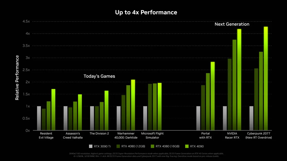
Based on Nvidia's benchmarks, it's going to be a mixed bag. The first three games in the above chart on the left don't use DLSS, or DLSS 3. The RTX 4080 12GB is often tied with or slightly slower than an RTX 3090 Ti when DLSS 3 and ray tracing aren't part of the equation. How often will that be the case on future games is far more difficult to predict.
In a lot of ways, the RTX 40-series launch so far feels very reminiscent of the RTX 20-series launch. Nvidia is once again hyping up ray tracing and DLSS, only we're now in round three of that story. The RT hardware is far more capable, DLSS 3 is supposed to be a lot better as well, but will all the big games support both technologies to sufficient levels? Undoubtedly the answer is no; some will, some won't.
Meanwhile, generational pricing has increased (again), and the specs on some of the models certainly look questionable. RTX 4080 12GB feels far too much like it really should have been the RTX 4070 right now, and Nvidia could have started tacking on Ti and Super or whatever to create other models.
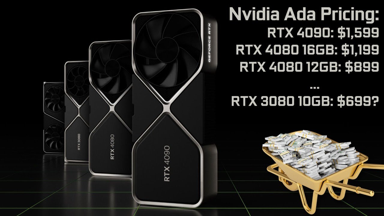
The RTX 3080 10GB will apparently still linger on with a $699 MSRP for the time being. That certainly can't last, not when an eventual RTX 4070 will inevitably displace it on performance and features. But Nvidia and its partners need the unwitting to buy up the existing inventory of RTX 30-series cards, for the highest prices they can still get, before they're ready to move down the stack to the rest of the Ada Lovelace lineup.
We're still waiting for full details on AMD's RDNA 3 lineup as well, and as discussed above, the design decisions AMD made — specifically with GPU chiplets — should result in lower prices that Nvidia can't possibly match. AMD may not take the outright performance crown, but if it can come close while undercutting Nvidia's prices, it might not matter. Add to that Intel's Arc A770 and A750, which could launch in the near future as well. We'll see who emerges as the victor in the GPU market in the next couple of months.
