X-NAND Technology Gets Patented, QLC Flash with SLC Speed
X-NAND chips could arrive very soon

During last year's virtual Flash Memory Summit 2020, the CEO of NEO Semiconductors, Andy Hsu, presented a novel NAND technology that will give us better speeds and higher destiny. Called X-NAND, the tech was at the time just a presentation. However, today the company finally got its designs approved and patented.
The X-NAND technology is a novel approach to NAND memory development, designed by NEO Semiconductor. NEO Semiconductor is a silicon valley company headquartered in San Jose, started in 2012. To date, the company has been granted more than 20 memory-related patents and has more in the works.
X-NAND technology aims to have the speeds of Single-Level Cell (SLC) NAND and deliver the capacity of Quad-Level Cell (QLC) NAND flash, all while trying to do it in the smallest form factor as possible. We delivered a detailed look at what the technology offers in our coverage here.
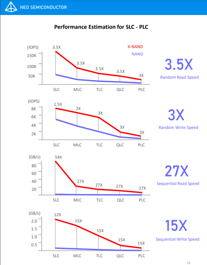
Article continues belowX-NAND is basically a combination of two worlds, where the technology uses bits from SLC and QLC to combine it into one high-endurance, high-speed, high-capacity NAND solution. Below, you can find NEO's performance estimation chart, highlighting the potential of its devices. To get a more in-depth look at all aspects, including density and endurance, please refer to the 16-page whitepaper available here.

We're in an era that demands capacious high-speed storage and X-NAND seems to be the perfect choice for expanding storage capacity and performance, with applications like 5G and AI/ML seeing the biggest improvements.
Neo doesn't manufacture chips based on X-NAND tech but rather just provides memory makers a blueprint to produce their own solutions. NEO Semiconductor hopes to license its X-NAND IP to some big memory makers like Samsung, SK Hynix, and Micron, where they would purchase the IP and just embed it into their offerings. This would result in better market adoption of X-NAND, as memory makers have the production capacity and wherewithal to push the new technology into the market.
Get Tom's Hardware's best news and in-depth reviews, straight to your inbox.
-
Alvar "Miles" Udell Cost needs to come down and density increase though in a hurry.Reply
This is the age of 4K120 and 8K30 professional cameras with consumer cell phones able to shoot 4K video along with the removal of the mSD slot (not that most mSD cards are able to keep up with 4K anyway), 128 and even 256GB storage doesn't get you far these days. -
cyrusfox How is this at all differentiated from what the manufacturers already all do on QLC based SSDs? All of them are already using a SLC cache to speed up the QLC NAND. Intel was the first to do it with the 660P and is on the third iteration with the 670P, Micron does it with the P1, Rocket as well. Is it a magically better implementation? Does it use dedicated SLC chips or the traditional style of every NAND chip is able to run in SLC mode until the drive starts filling up then you get a lower and lower amount of SLC capable cache.Reply
If my memory serves me, a lot of the SSD manufacturers where enabling software cache dram to help speed up as well for those with the spare memory. I wish this company luck but from this announcement I don't see how their solution already beats the first party one, or what value they really offer unless they are also designing cutting edge controllers.