APC BGE90M-CA UPS Tear-Down
What Difference Does It Make?
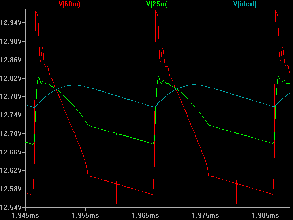
A picture is worth a thousand words, so I fired up LTSpice and did a quick mock-up of a flyback circuit. In red, you have the output waveform using a capacitor with 60mΩ of ESR, which looks quite similar to what we saw across the Lelon capacitor. In green, we have an ESR of 25mΩ (typically in the form of two smaller devices in parallel) teamed with a 10µF MLCC to handle the high frequency content, as you will often find in higher-quality designs. If we could buy an ideal capacitor and put it in, we would get the cyan waveform. My mock circuit operates in open loop with a 10Ω load, and the differences in DC offsets are representative of reduced capacitor losses, meaning the 25mΩ and ideal capacitors make the circuit about 1.7% and 3% more efficient, respectively.
Every time you buy a device containing a power supply where manufacturers shaved pennies on capacitors, this is one of many compromises being made.
Analog And Digital Support
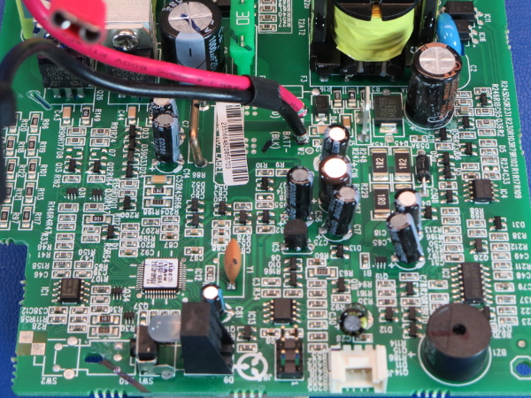
There is not much to get excited about on this half of the board: operational amplifier, linear regulators, tons of surface mount resistors, capacitors, diodes and transistors, a handful of Chang capacitors, and a 48-pin QFP micro-controller with a sticker identifying the firmware as “REV1 ©2011.” Just above the USB board header, between the bi-color (red/green) LED and buzzer, sits a lone OST 25V 22µF capacitor.
Article continues belowIf you weren’t counting, that’s four capacitor brands so far, all on the lower half of the reputation ladder.
The Business End – Primary Side
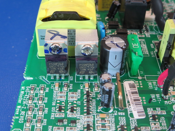
The inverter involves a rather large chunk of the board, starting with the battery, the 30A battery fuse, a current measurement shunt (the thick piece of wire below the large capacitor), a CapXon 1000µF 25V capacitor to provide bypassing, and the DC-DC boost converter’s ST P55NF06 (60V/50A/18mΩ) FETs driving the boost transformer in a double-forward topology.
Just as it was on the AC input and output monitoring side, the boost converter’s DC output voltage gets sensed through a resistor network, this one tucked away along the bottom-left edge.
The Business End – Secondary Side
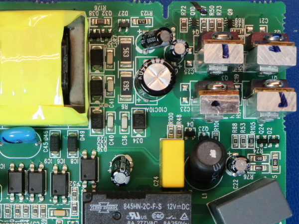
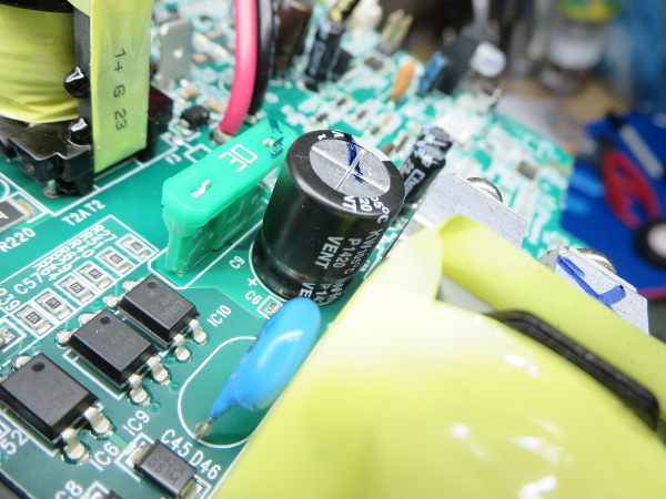
On the output side, we have a discrete diode bridge with snubber capacitors charging an OST RLG 450V 4.7µF capacitor, a handful of support components generating gate drive voltages for the output IRF610 (200V/3.3A/1.5Ω) FET bridge and their control opto-couplers, followed by an inductor and 100nF X-class capacitor providing some degree of output filtering. I do not like that OST capacitor’s survival chances: there is no inductor on the output of this double-forward converter, which means that the capacitor will get subjected to some harsh ripple current.
Get Tom's Hardware's best news and in-depth reviews, straight to your inbox.
There you go, the internal tour is complete. This is another fine example of a generally great design brought down a few pegs to save $0.50 on parts.
How Electronic Inverters Work
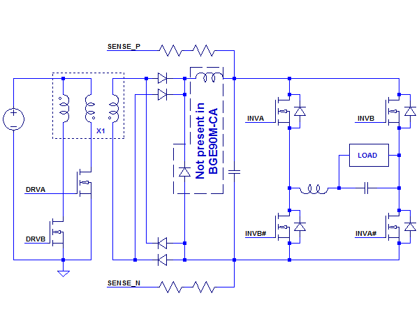
In a nutshell, electronic inverters work by doing about the same thing a typical power supply does, but in reverse. Instead of taking line voltage, rectifying it, stepping it down through a high-frequency transformer and rectifying it again, DC voltage gets turned to AC through the high-frequency step-up transformer, rectified to HVDC, turned into line-voltage AC by the FET bridge operating in diagonally opposite pairs, and then lightly filtered across the load.
With fast enough FETs, it would be possible to use the exact same circuit to generate arbitrary waveforms by adding the appropriate modulation to either the top or bottom FETs, exactly as the CP1000AVRLCD did with its transformer.
Idle Efficiency
Why bother with the complexity? Because electronic inverters are far more efficient at light loads than iron-core inverters are. When there is no load, they top off their output capacitors and that’s it. Iron core transformers, on the other hand, have a significant magnetizing current that they require regardless of load. At light loads, this accounts for the bulk of the power draw.
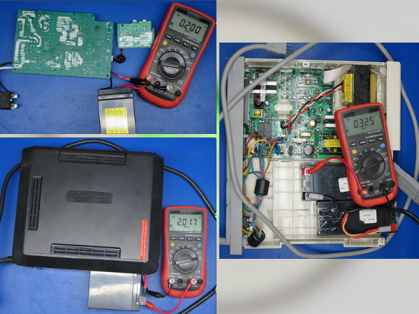
I put my multimeter in series with my spare UPS’ batteries to have a look at their respective current draw with no external load attached. The BGE drew 200mA and could theoretically keep going for over 20 hours, while the CP drew 2A and would go dead doing nothing within four hours (despite having a 33%-larger battery). Am I being unfair by comparing a 125VA UPS to a 1000VA one? Not really: my ancient BX1000’s inverter still works correctly and it drew 325mA at 24V, less than a third of CP’s power.
Standby Power
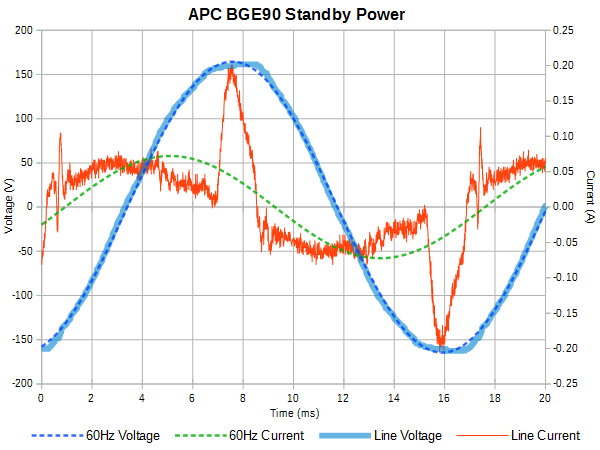
With the unit off (charger only), the BGE90 draws 2.5W and 6VA versus 3.5W and 8.3VA in normal standby operation, which is 700mW worse than the BE550’s 2.8W and 5.6VA in standby. At first, you may wonder why APC could not be bothered to put a more efficient standby supply in there. But then again, this UPS does have a pair of USB ports with a combined maximum output of 2.5A powered by a DC-DC converter, which means that the standby supply also needs to power the 12.5W USB outputs.
Do Not Try This At Home
If you thought that using a UPS after a power strip was cringe-inducing, fasten your seat belts and hold on to your hats!
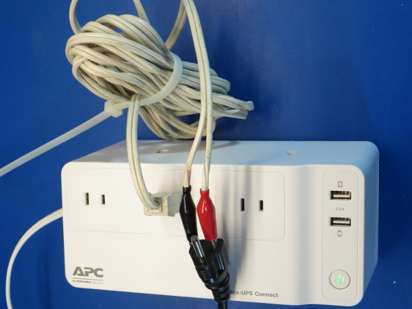
When I got around to looking at output waveforms, I ran into a little issue: the BGE90 is not intended for running devices that require grounding, and therefore only has two-pin polarized outlets. I used my simple and unsafe “universal lamp cord to alligator clip adapter” to get around this safety measure.
This is actually small-fry stuff compared to earlier in the piece when I had my hands millimeters from a live PCB.
Output Waveform
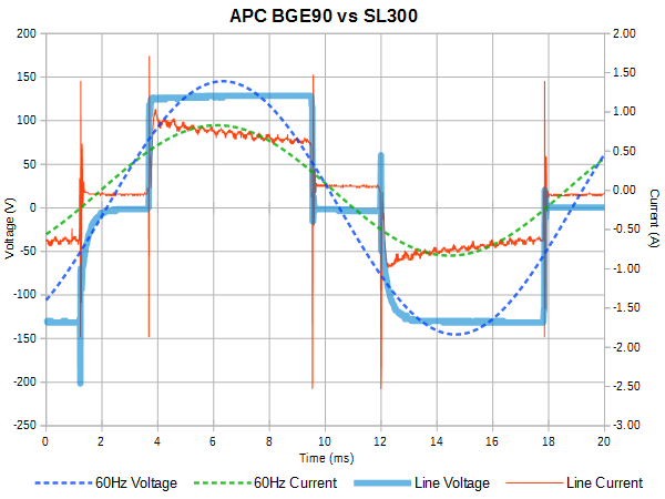
Instead of the 160-180V flats seen previously, the BGE90 only outputs 130V while delivering 64W, which seems a little low. Factor in the 72% duty cycle shown here, and the effective output voltage becomes 107VRMS. In the THD department, this waveform scores a surprisingly good 27% while under load. I added extra loads to see if I could cause an overload condition, but ran out of outlets at 88W, 13W over the specification and definitely more than sufficient to run the modem, router, and ATA it's primarily intended for.
I can think of at least one advantage to such a low peak voltage waveform: many small power adapters are still linear (use iron core transformers), where the lower voltage reduces the amount of power loss within them.
It Needs To Be About 20% Cooler
There aren’t many bad things to say about the BGE90M-CA. Its mechanical construction is sound except for the loose battery compartment, the wire gauges and breaker are in line with what the unit is intended for, and the board layout and assembly quality are as clean as they come. The single biggest issue is APC's choice of third- and fourth-tier capacitor companies, especially that lone Lelon eating the output of the UPS’ flyback power supply. I was thinking of buying type-A to barrel cables to power my modem and telephony adapter from the USB power ports, but if I did that, I doubt the Lelon capacitor would survive more than a year of 24/7 ripple exposure. Does that sound like a dare or a challenge?
In all seriousness, that 3.5W the unit is dissipating with nearly no ventilation does cause it to become noticeably warm, and I’m certain APC could have reduced its standby power consumption by more than 20% with a few design tweaks. Just look at the BE550G’s 2.8W.
Those two potential sore points aside, it should be one handy little UPS to have.
MORE: CyberPower CP1000PFCLCD Tear-Down
MORE: APC BE550G Tear-Down
MORE: Tripp-Lite SMART1000LCD Tear-Down
Follow us on Facebook, Google+, RSS, Twitter and YouTube.
-
gamebrigada For 30 bucks I'm not super concerned about the capacitors. The soldering job is decent and not done by a shmuck, and the board is nicely designed and doesn't look like it was designed by a 5 year old. Low quality capacitors scare me less than a potential fire.Reply -
nukemaster Another good read.Reply
Thanks.
I looked at this(something from the same family at least) for a cordless phone backup/router/ect, but slightly larger units did not cost much more. I did not see these for 30 dollars in my area. -
Daniel Sauvageau Reply
You're welcome!18333740 said:Another good read.
Thanks.
$30 was a clearance sale price. These units were manufactured in 2014, someone must have discovered pallets worth of these in the back of a warehouse somewhere and wanted to get rid of stale stock. At $30, these were almost worth getting just to scavenge the battery. The regular retail price is $47. While I was proofreading Chris' edits, I noticed the Newegg(.com) banner advertising a BGE90 for $80. I don't see stuff being so much cheaper in Canada than the USA very often. At such a large price discrepancy, it is almost worth it for US residents to order these units from Canada even before accounting for the exchange rate.18333740 said:I looked at this(something from the same family at least) for a cordless phone backup/router/ect, but slightly larger units did not cost much more. I did not see these for 30 dollars in my area.
New 600-650VA variants of this unit (BE600M1 and BN650M1) were launched last month (June 2016) and are only a few centimeters longer. They do cost $90-100 CAN though and at that price, it may make more sense on my side of the border to buy a pair of BGE90Ms and split the load.
BTW, there was an 8h long power outage at my mother's place due to trees shorting power lines out during a severe thunderstorm last week. The BE550G held out for about 2h30, twice as long as I was expecting it to based on its packaging's runtime chart. I'm glad it held up so much longer than planned since my mother waited until about 1h30 into the outage before calling me. The battery should have been dead by then based on the chart. Apparently, I hadn't made it clear enough the first time around before I set her up with VoIP to save her $40/month on phone bills that one key disadvantage of a VoIP setup is that dead UPS battery = no internet = no phone so if she waits to call, she may no longer be able to do so by the time she decides to. Maybe I should replace the 550 with a Frankenstein BGE90 connected to an external 12AH battery, should last over 10 hours. If voip.ms has a feature to send an email or call a number when an account fails to register for more than 15 minutes, I need to set that up. -
razor512 Why aren't they giving these devices li-ion batteries? The whole thing is lower drain, thus no super high end battery is needed to handle a very high current.Reply -
Daniel Sauvageau Reply
Lead-acid batteries are cheaper and can safely tolerate a whole lot more abuse than lithium cells do.18334228 said:Why aren't they giving these devices li-ion batteries?
-
alextheblue Reply18333740 said:BTW, there was an 8h long power outage at my mother's place due to trees shorting power lines out during a severe thunderstorm last week. The BE550G held out for about 2h30, twice as long as I was expecting it to based on its packaging's runtime chart. I'm glad it held up so much longer than planned since my mother waited until about 1h30 into the outage before calling me. The battery should have been dead by then based on the chart. Apparently, I hadn't made it clear enough the first time around before I set her up with VoIP to save her $40/month on phone bills that one key disadvantage of a VoIP setup is that dead UPS battery = no internet = no phone so if she waits to call, she may no longer be able to do so by the time she decides to. Maybe I should replace the 550 with a Frankenstein BGE90 connected to an external 12AH battery, should last over 10 hours. If voip.ms has a feature to send an email or call a number when an account fails to register for more than 15 minutes, I need to set that up.
It would be so much more efficient to be able to use a DC UPS though. Maybe get a 12V DC UPS and a couple of DC-DC adapters? :P -
Daniel Sauvageau Reply
I have entertained that idea a few times. The biggest hassle is getting the correct barrel connectors for everything you might want to connect to such an UPS and make sure you don't get leads mixed up between voltages and devices if you have devices that cannot tolerate 14V on their power input: if you have multiple 5x1.6mm barrel connector leads split between 5V devices and 12V devices, it would be quite easy to accidentally use the wrong lead on a 5V device and blow it up. I suspect this is the main reason why proper DC UPSes aren't widely available despite enabling much higher overall efficiency.18339557 said:It would be so much more efficient to be able to use a DC UPS though. Maybe get a 12V DC UPS and a couple of DC-DC adapters? :P
In principle, all you'd need to put one together for 30W worth of loads is a 3A 13V power supply to act as a float charger for the SLA battery with all the 12V loads connected to the battery and 5V USB adapters with sufficient output current for all the 5V stuff. -
alidan Reply18334174 said:
You're welcome!18333740 said:Another good read.
Thanks.
$30 was a clearance sale price. These units were manufactured in 2014, someone must have discovered pallets worth of these in the back of a warehouse somewhere and wanted to get rid of stale stock. At $30, these were almost worth getting just to scavenge the battery. The regular retail price is $47. While I was proofreading Chris' edits, I noticed the Newegg(.com) banner advertising a BGE90 for $80. I don't see stuff being so much cheaper in Canada than the USA very often. At such a large price discrepancy, it is almost worth it for US residents to order these units from Canada even before accounting for the exchange rate.18333740 said:I looked at this(something from the same family at least) for a cordless phone backup/router/ect, but slightly larger units did not cost much more. I did not see these for 30 dollars in my area.
New 600-650VA variants of this unit (BE600M1 and BN650M1) were launched last month (June 2016) and are only a few centimeters longer. They do cost $90-100 CAN though and at that price, it may make more sense on my side of the border to buy a pair of BGE90Ms and split the load.
BTW, there was an 8h long power outage at my mother's place due to trees shorting power lines out during a severe thunderstorm last week. The BE550G held out for about 2h30, twice as long as I was expecting it to based on its packaging's runtime chart. I'm glad it held up so much longer than planned since my mother waited until about 1h30 into the outage before calling me. The battery should have been dead by then based on the chart. Apparently, I hadn't made it clear enough the first time around before I set her up with VoIP to save her $40/month on phone bills that one key disadvantage of a VoIP setup is that dead UPS battery = no internet = no phone so if she waits to call, she may no longer be able to do so by the time she decides to. Maybe I should replace the 550 with a Frankenstein BGE90 connected to an external 12AH battery, should last over 10 hours. If voip.ms has a feature to send an email or call a number when an account fails to register for more than 15 minutes, I need to set that up.
have a costco where i live, they have 810 watt upses there for 100$ forget the brand name but remember them being good. if this costs 80 and the 810 costs 100, may as well get the significantly better one. -
Daniel Sauvageau Reply
If your objective is very long runtime, getting a massively higher VA rating UPS may not necessarily do you any good: in a traditional transformer-based inverter (every UPS I have shown here so far other than the BGE90 and BX1000), a larger transformer core means higher magnetizing current and other related losses which bleed off battery power. When I measured the CP1000AVRLCD, BX1000 and BGE90's no-load battery current draw, I got ~25W for the CP, ~7W for the BX1000 and ~2.5W for the BGE.18349342 said:have a costco where i live, they have 810 watt upses there for 100$ forget the brand name but remember them being good. if this costs 80 and the 810 costs 100, may as well get the significantly better one.
If your 810W UPS uses a traditional transformer-based inverter like the 1000AVRLCD does, it will need a battery about twice the size of the BGE90's to beat it at endurance on 10-15W loads due to wasting more power walking its large transformer core through its hysteresis loop than actually powering the loads.
Sometimes, less is more. The typical use-case for the BGE90 should be one of those cases when compared against UPSes using traditional inverters. -
alextheblue Reply18342170 said:
I have entertained that idea a few times. The biggest hassle is getting the correct barrel connectors for everything you might want to connect to such an UPS and make sure you don't get leads mixed up between voltages and devices if you have devices that cannot tolerate 14V on their power input: if you have multiple 5x1.6mm barrel connector leads split between 5V devices and 12V devices, it would be quite easy to accidentally use the wrong lead on a 5V device and blow it up. I suspect this is the main reason why proper DC UPSes aren't widely available despite enabling much higher overall efficiency.18339557 said:It would be so much more efficient to be able to use a DC UPS though. Maybe get a 12V DC UPS and a couple of DC-DC adapters? :P
In principle, all you'd need to put one together for 30W worth of loads is a 3A 13V power supply to act as a float charger for the SLA battery with all the 12V loads connected to the battery and 5V USB adapters with sufficient output current for all the 5V stuff.
Change the connectors on the units in question or glue them in and cut the cord, adding a second connector (something akin to a breakaway connector on an Xbox 360) that's different and incompatible for each device :P
Really I think that all small widgets and whatsits should just go USB Type C. :D Then it would be not only viable, but really easy. Heck at that point you'd basically be building a really high-class USB power bank.
