Making Lemonade: Overclocking Your Locked AMD Processor
Get Tom's Hardware's best news and in-depth reviews, straight to your inbox.
You are now subscribed
Your newsletter sign-up was successful
Overclocking Via The BIOS
BIOS Overclocking
In each overclocking scenario, we first disabled Cool’n’Quiet, C1E, and spread spectrum in the BIOS.
This isn’t completely necessary, but taking the time to determine the maximum reference clock can be valuable later when dissecting the reasons behind a failed overclock. To do this, you normally lower the CPU, NB, and HT multipliers as well as the memory frequency way down to eliminate any of the resulting frequencies from limiting headroom. The reference clock is then increased in small increments and testing is done along the way to ensure stability. In the 790FX-GD70 BIOS, MSI uses a CPU FSB frequency setting that refers to AMD’s HT reference clock.
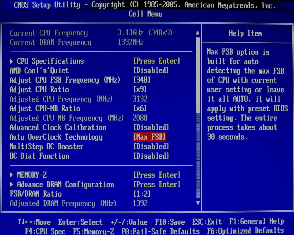
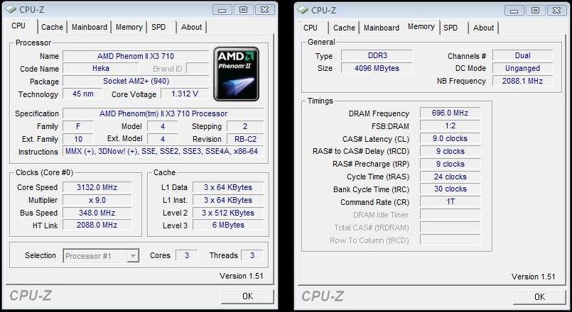
This was initially the plan, but first we wanted to see what the Auto Overclock BIOS option could do to the default setting of 200 MHz. We set this option to Find Max FSB and saved the BIOS changes. The system then ran through a short series of restart cycles and after about 20 seconds booted up at an impressive 348 MHz reference clock!
After successfully confirming system stability at these settings, we knew the reference clock wouldn’t be a limitation with this CPU and motherboard combination.
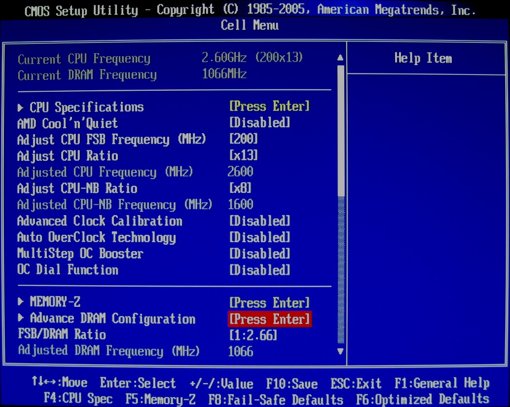
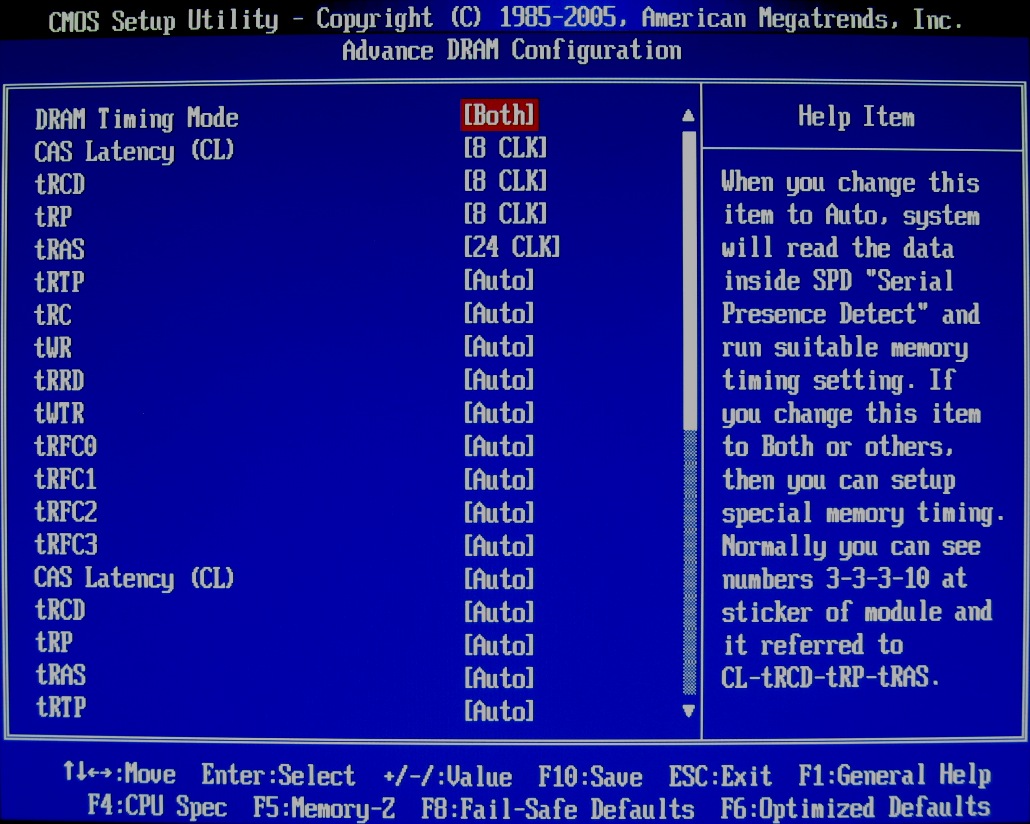
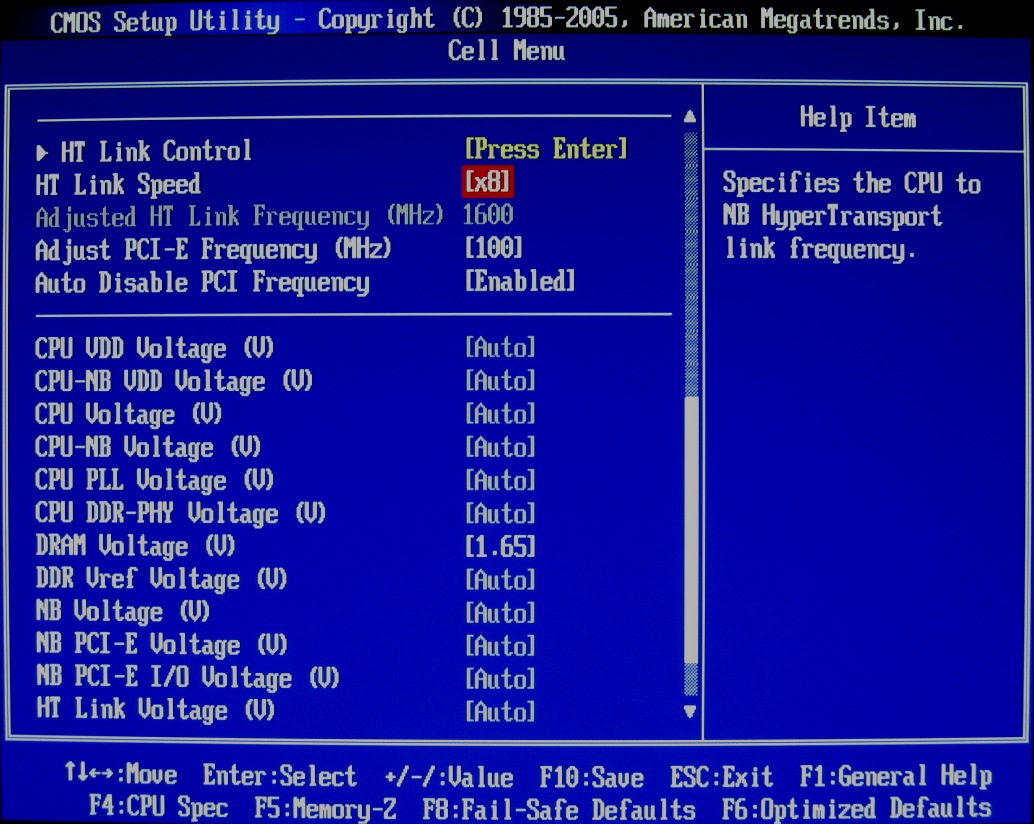
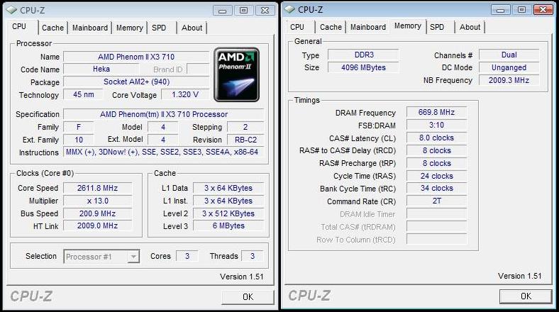
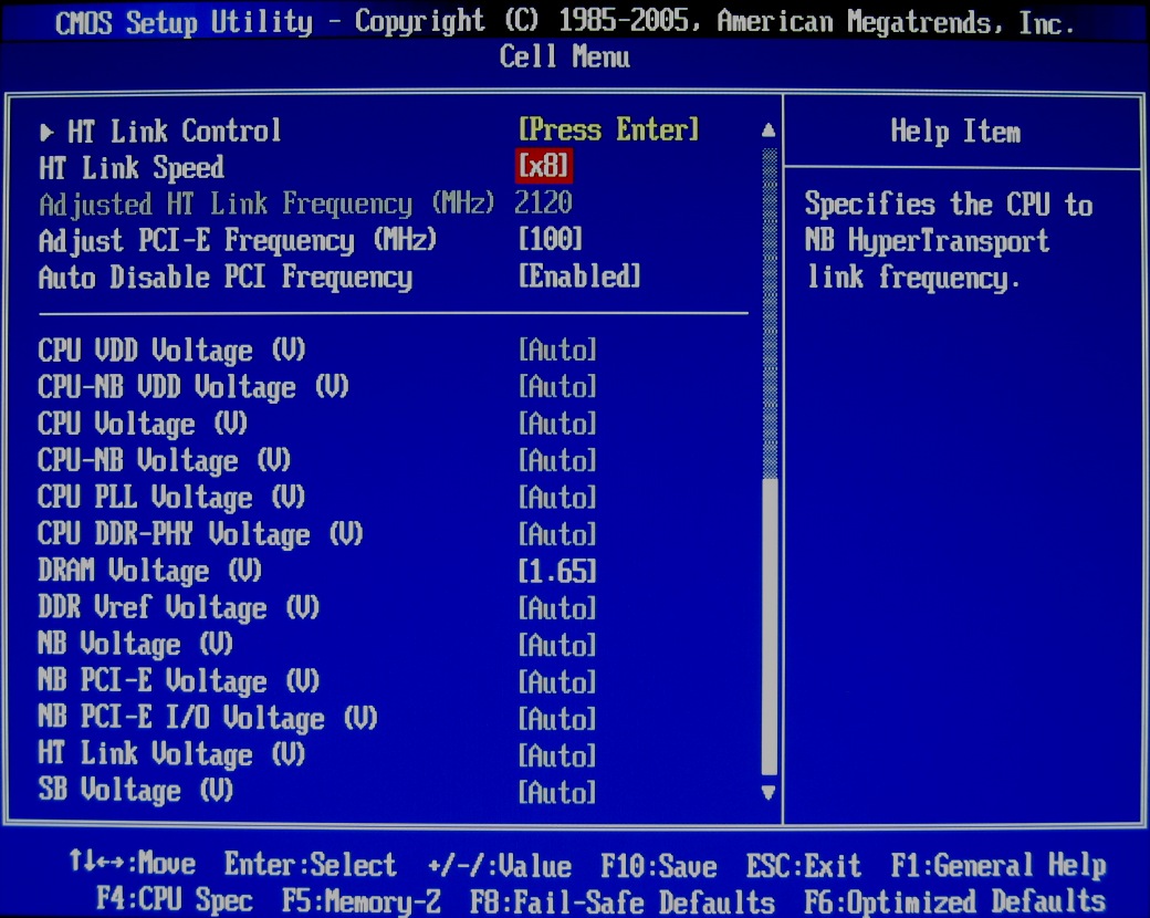
Now it was time to start overclocking the processor. In the Cell menu, we set values back to defaults. Then we set the CPU-Northbridge ratio and HT Link speed to an 8x multiplier. The FSB/DRAM ratio was lowered to 1:2.66 and memory timings were manually set to 8-8-8-24 2T.
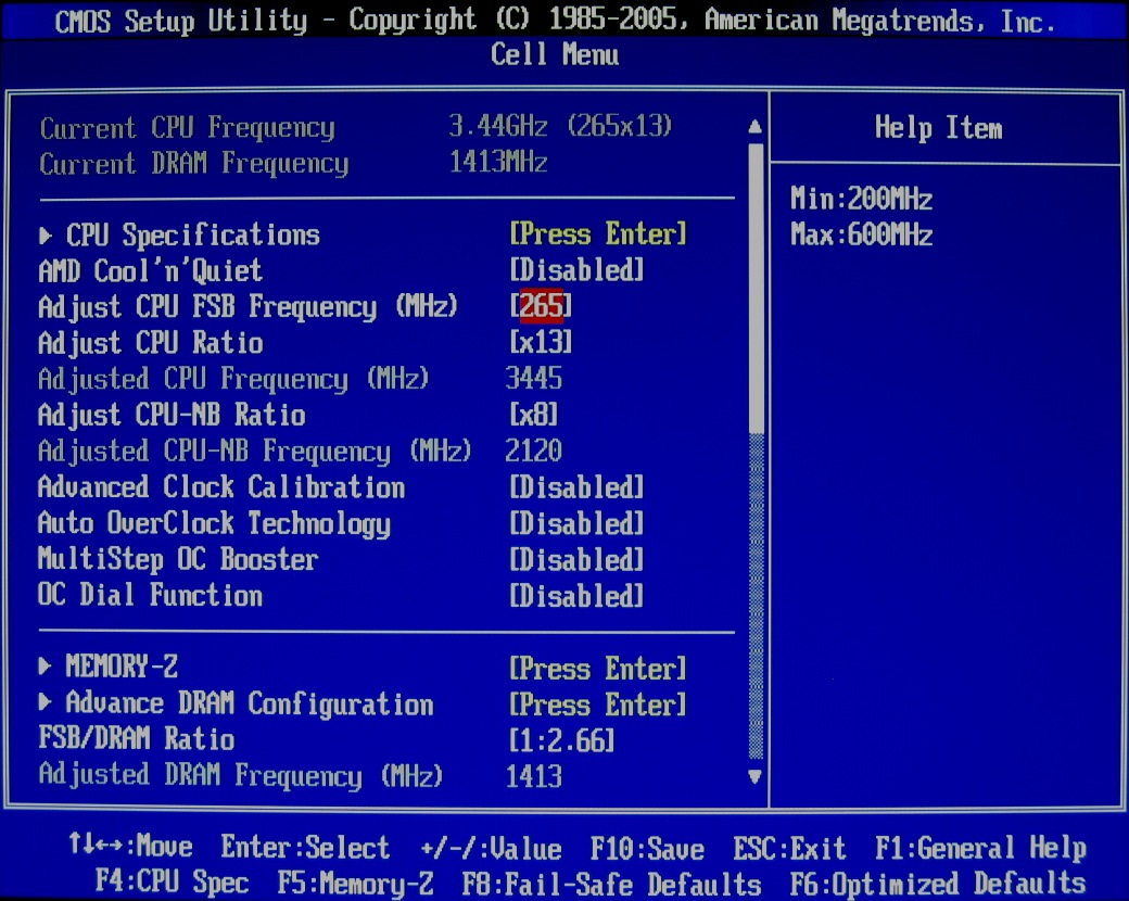
Already knowing this CPU was stable at 3.13 GHz (348 x 9), we jumped right to a 240 MHz reference clock and successfully ran stability testing. We then increased the reference clock in 5 MHz increments and stability tested at each frequency. The highest it would go at stock voltage was 265 MHz, resulting in an impressive maximum stock voltage overclock of 3,444 MHz.
Get Tom's Hardware's best news and in-depth reviews, straight to your inbox.
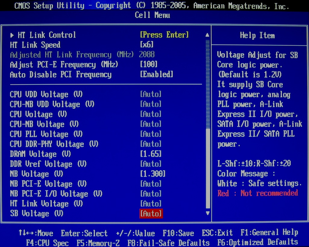
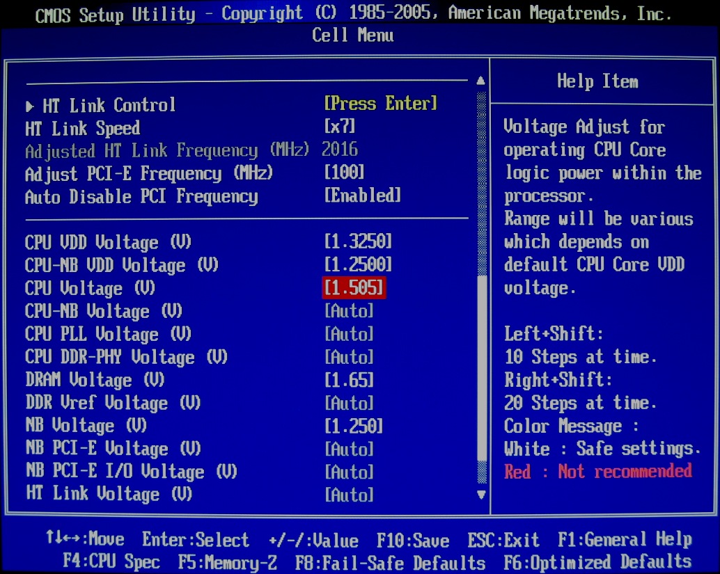
Lowering the HT Multiplier setting to 7x did not aid in further overclocking, so it was time to raise voltages. As mentioned above, the CPU Voltage ID is locked from going higher than 1.325V, so the CPU VDD voltage range available in the BIOS is 1.000V-1.325V, or Auto. But the board’s CPU voltage can still be raised by applying an offset on top of the CPU VID. Offset is adjusted in the BIOS as CPU voltage, and available values at this processor’s 1.325V VDD are 1.005–1.955V.
At a fairly tame CPU voltage of 1.405V, the reference clock was raised 5 MHz incrementally, maxing out at a stable 280 MHz and resulting in a 3,640 MHz core speed, 1,960 MHz HT Link speed, 2,240 MHz northbridge speed, and 1,493 MHz DDR3. This would be great for long-term 24x7 use, but come on. We should be able to do better than that for today’s endeavors!
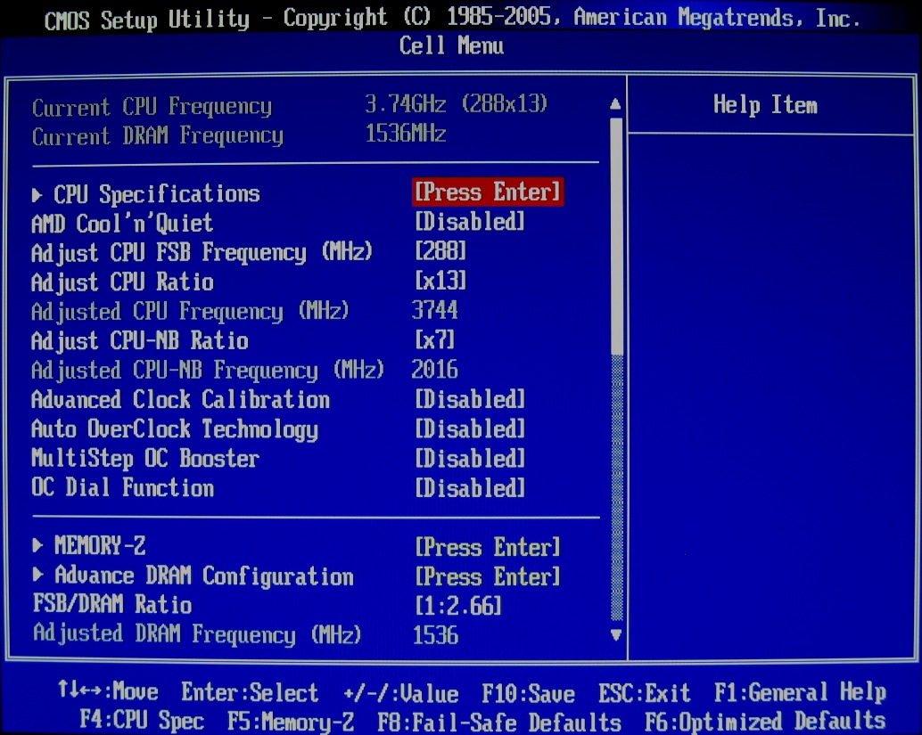
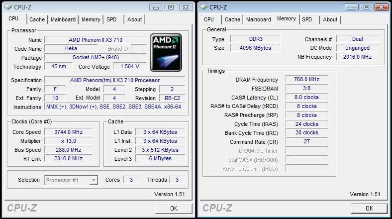
We pressed on, lowering the northbridge multiplier to 7x and bumping the CPU voltage to 1.505V. For reference, the actual CPU voltage dropped to 1.488V during load testing. At this voltage, the Phenom II X3 710 reached a stable 3,744 MHz at a 288 MHz reference clock. In our open-air bench system, the CPU temperature during Prime95 testing now hovered around 49 degrees Celsius, or 25 degrees above ambient room temperature.
Current page: Overclocking Via The BIOS
Prev Page Introduction Next Page Overclocking Via AMD OverDrive-
sohei it's about how to squeeze all performance from an locked cpu .Reply
this is a pro' article (head shot) -
brisingamen great article, should be more like it,Reply
and a few more gaming benches wouldnt hurt either guys!
speaking of headshots yes unreal tournament is probably the most important game to exemplify the value of overclocking and added framerates due to "headshots" and shtuff.
keep up the good work! -
Onus stray_gatorWhat's the point of using a high-end mobo to overclock a mainstream/value cpu?Fair question; no one would likely do this IRL, but I think the point here was to see how high the locked CPU could go, so they used a premium mobo.Reply
Paul, now that we know what this specific CPU can do, would it be useful to now put it on a more typical mainstream mobo and see what one might get from the same chip under more typical conditions?
The point would be to answer the following: if my budget just grew by $25, does it make more sense to buy a BE CPU or to get a more premium mobo? -
haplo602 stray_gatorWhat's the point of using a high-end mobo to overclock a mainstream/value cpu?Reply
because value mobos vary in stability much more than premium mobos. this article was just about the CPU limit, not the mobo limit. -
Tom's should do a shoot-out between an i7 920 and a 965BE that's had the multiplier taken down to 13x(2.6ghz), then both OCed to the max on the northbridge alone. I'm sure that would close the gap atleast somewhat, but I'm interested to see exactly how much. Maybe they could screw around with the HyperTransport multiplier as well, it might turn out that AMD has been shooting itself in the foot with the unlocked multiplier, when more performance would be had if they were forcing people to use the northbridge.Reply
-
Shadow703793 Good write up; but PLEASE do NOT recommend OCing via Windows. Most pro's here will tell you that same thing. BIOS > Windows for OCing.Reply
