Nvidia GeForce GTX 275 Preview: A Well-Timed Retaliatory Strike?
The GeForce GTX 275’s Inner Workings
As mentioned on the page prior, Nvidia’s GeForce GTX 275 is most easily thought of as half of a GeForce GTX 295. It employs the same 55 nm version of the GT200 graphics processor and includes 240 shader cores and 80 texture address/filtering units, just like the higher-end GeForce GTX 285.
Nvidia differentiates the two single-GPU solutions by disabling one of the GTX 275’s ROP/frame buffer partitions, yielding a total of 28 ROPs and an aggregate 448-bit pathway to 896 MB of GDDR3 memory. Given the timing and power improvements that we discussed with Nvidia when it launched GTX 295, we’d expect this new board to consequently use less power than the GTX 285. But as we’ll see in the power consumption chart, that’s that not necessarily an absolute. One more hint that this card centers on the 55 nm chip, though: whereas the 65 nm GeForce GTX 280 required one eight-pin and one six-pin power connector, the GTX 275 (like the 285) gets by with two six-pin PCIe connectors instead.
Clock speeds on the GeForce GTX 275 are down just slightly from what you’d find on a GTX 285, but higher than the same components on a GTX 295 board, presumably as a result of only needing to cool one GPU and 896 MB of memory instead of two chips plus 1,792 MB. The GeForce GTX 275’s core runs at 633 MHz (versus GTX 285’s 648 MHz). Its shader clock is set to 1,404 MHz (versus 1,476 MHz). And its GDDR3 memory modules run at 1,134 MHz (compared to 1,242 MHz on a stock GTX 285).
| Header Cell - Column 0 | GeForce GTX 285 | GeForce GTX 275 | GeForce GTX 260 Core 216 | Radeon HD 4890 | Radeon HD 4870 |
|---|---|---|---|---|---|
| Manufacturing Process | 55 nm TSMC | 55 nm TSMC | 55 / 65 nm TSMC | 55 nm TSMC | 55 nm TSMC |
| SPs | 240 | 240 | 216 | 800 | 800 |
| Core Clock | 648 MHz | 633 MHz | 576 MHz | 850 MHz | 750 MHz |
| Shader Clock | 1,476 MHz | 1,404 MHz | 1,242 MHz | 850 MHz | 750 MHz |
| Memory Clock | 1,242 MHz GDDR3 | 1,134 MHz GDDR3 | 999 MHz GDDR3 | 975 MHz GDDR5 | 900 MHz GDDR5 |
| Frame Buffer | 1 GB | 896 MB | 896 MB | 1 GB | 1 GB / 512 MB |
| Memory Bus Width | 512-bit | 448-bit | 448-bit | 256-bit | 256-bit |
| ROPs | 32 | 28 | 28 | 16 | 16 |
| Price | $340 | ~$249 | $180 | ~$249 | $180 |
A Familiar Form Factor
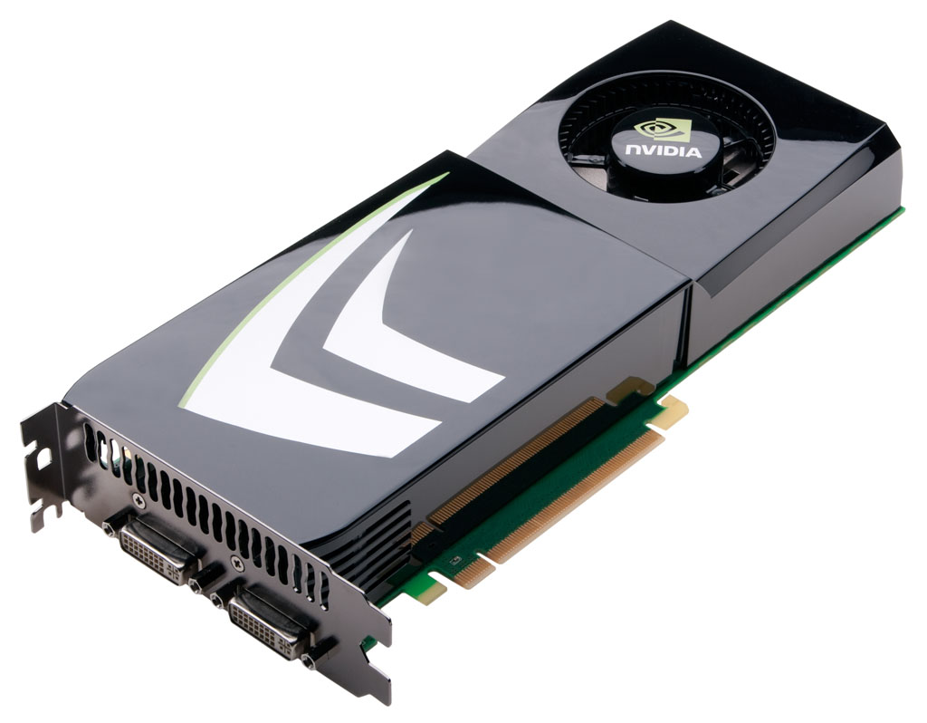
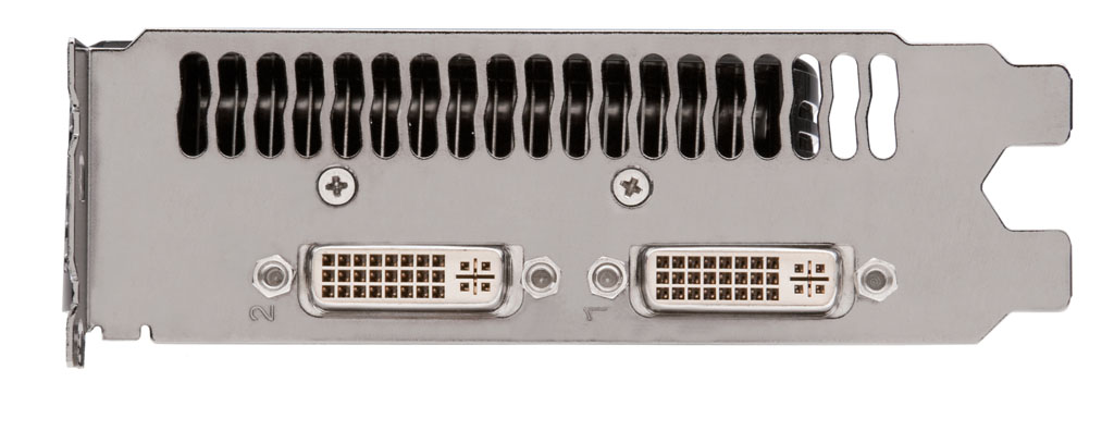
While a GeForce GTX 285 gives you two dual-link DVI and one component output, The GeForce GTX 275 is limited to the two digital connectors—fine by us really, given the growing prevalence of HDMI.
The card itself should look very familiar. It’s based on the same 10.5” PCB design used by Nvidia’s other dual-slot boards, like the GTX 260 Core 216 and GTX 285. While each of the three cards employs slight layout variations, system builders must certainly appreciate the somewhat-standardized dimensions.
It’s also worth noting that, even under load, the GTX 275’s blower is remarkably quiet—quieter on our test bench than the 120 mm fan on our Thermalright Ultra 120 Extreme CPU cooler, in fact.
Get Tom's Hardware's best news and in-depth reviews, straight to your inbox.
Current page: The GeForce GTX 275’s Inner Workings
Prev Page Introduction Next Page Still Waiting On A Killer PhysX App?-
privardo This would be my good price, good performance and the right time upgrade from 8800 GTS 512mb. Thanks for this awesome review!Reply -
eklipz330 i think putting the competitors next to eachother would have been easier on the eyes... putting 4870x2 gtx295 next to eachother, 4890 gtx275 next to eachother...you catch my driftReply -
cangelini Yeah, but with each resolution its own color, after looking at it both ways, it was easier to put each product family in descending order--hopefully it makes just as much sense that way!Reply -
eklipz330 srry for dp butkudos to nvidia for stepping up their game in the last second that had nothing to do with renaming cards. an attractive card at an attractive price.Reply
it'd be smart for ati to not release the 4890x2. wouldn't make any sense, like my grammar skills. hopefully drivers can catch up and do some damage, id doubt they woudl do anything dramatic though. -
megamanx00 Too bad they didn't overclock the 4890 and the 275 for the review. I would have liked to have seen how the two cards compared overclocked. The heat and power dissipation on the 4890 would probably be a little scary though :D.Reply -
megamanx00 I think the big thing for nVidia now is, who's going to spend money on a 285 with the 275 so close?Reply -
cangelini megamanx00Too bad they didn't overclock the 4890 and the 275 for the review. I would have liked to have seen how the two cards compared overclocked. The heat and power dissipation on the 4890 would probably be a little scary though .Reply
No need to fuel the tin-foil brigade elsewhere on the Web re: hand-picked cards. When we can get our hands on these boards for our System Builder Marathons, straight from e-tail, then we'll give you the goods on overclocking with the same boards available to everyone else! -
privardo ReplyOriginally we said that the price would be $249 in the US, and €249 in Europe, however if the Euros-to-USD conversion is correct (1.00 Euro = 1.31 U.S. Dollars), the North American version should cost $327 instead.
If the retail price for this card is turn to be over $300, they will never fool this monkey cause he will just get two HD 4770 and crossfire'd them, which surely beat a single 275 -
privardo Reply"Originally we said that the price would be $249 in the US, and €249 in Europe, however if the Euros-to-USD conversion is correct (1.00 Euro = 1.31 U.S. Dollars), the North American version should cost $327 instead."
If the retail price for this card is turn to be over $300, they will never fool this monkey cause he will just get two HD 4770 and crossfire'd them, which surely beat a single 275 -
ifko_pifko Well... summing all the framerates is just nonsense. ;-) The games with higher fps will weigh more than the others. (I know that in this test the variance in fps is not as wide as in tests with more games, but keep that in mind in the future please and learn the basics of statistics... )Reply


