Z87 Hits The High End: Four Sub-$300 Motherboards
Situated barely below the priciest premium boards, which typically exceed $300, high-end Z87 Express-based motherboards offer enthusiasts almost everything they could want except for three-way SLI support. We put four of these platforms to the test.
Z87X-UD5H Firmware
Why you can trust Tom's Hardware
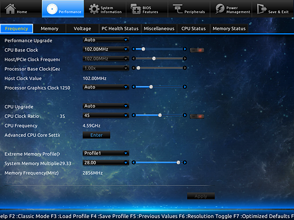
Gigabyte still uses its familiar high-resolution GUI for firmware settings, but a press of the F6 key allows us to zoom.
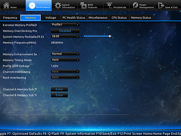
Frequency, Memory, and Voltage get separate tabs, where the Frequency tab controls base clock, CPU core, integrated GPU, and DRAM ratios. Though our CPU reached the same 4.59 GHz frequency as Asus' competing Maximus VI Formula, our DRAM was only stable up to DDR3-2800. Since Haswell’s maximum functional ratio gives us DDR3-2933 at a stock base clock, the board would have automatically added 2.3 MHz to the CPU base clock.


All multiplier-based overclocking relies on Intel's Turbo Boost functionality, though disabling Turbo Boost allows the Z87X-UD5H to lock a fixed multiplier ratio and turn off certain power-saving features. Other power settings must be manually configured to completely lock-in a specific voltage.
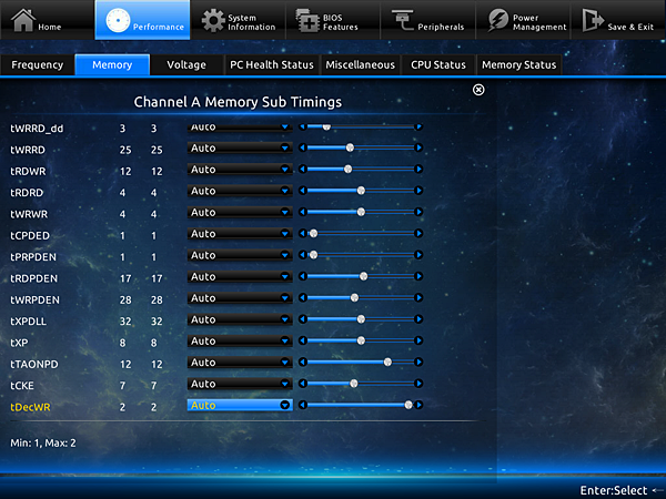
DRAM timings can be configured as all-channels (Manual) or in per-channel (advanced manual) mode. Memory profile and ratio settings are repeated from the frequency menu.


Each timing can be individually selected without disabling automatic mode for other timings.


Gigabyte loves submenus, so we need to jump through several pages to set up our basic overclocking parameters. Beyond those, we could also alter voltage droop compensation, power, and thermal limits through the Z87X-UD5H Advanced Power Settings menu.


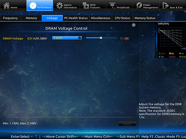
Three more pages of submenus give us CPU, DRAM, and PCH voltage control. We had to select 1.23 V to reach an actual 1.25 V core at or near idle, and core voltage still climbed to around 1.268 V under load. Higher voltage settings allowed the maximum core voltage to climb to a thermally-triggered throttle-inducing 1.27x volts. Similarly, a 1.635 V DRAM setting took us a few millivolts past our actual 1.65 V target. Actual voltage levels were verified with a voltmeter.
Get Tom's Hardware's best news and in-depth reviews, straight to your inbox.
-
vipervoid1 Reviewer seems like not really like MSI ~Reply
Always favoring Asus, ASRock and Gigabyte ~
No matter how less differences between each board ~
MSI Motherboard , the reviewer never have comment ~
I am a MSI brand fans , I admitted it , but the reviewer seems like ignored MSI's afford. -
slicedtoad Haswell motherboard guide: pick whichever looks best and has the right I/O. Performance-wise, they're all the same.Reply -
Crashman Reply
In the award contest between MSI and Gigabyte, Gigabyte would have probably won the award. The problem for Gigabyte is that it's new price is too cheap to compete in a $220-300 roundup.11638734 said:Reviewer seems like not really like MSI ~
Always favoring Asus, ASRock and Gigabyte ~
No matter how less differences between each board ~
MSI Motherboard , the reviewer never have comment ~
I am a MSI brand fans , I admitted it , but the reviewer seems like ignored MSI's afford.
Let's take a look at the article:11638739 said:And also dont have MSI software feature in the review ~
The Z87 MPower Max comes with the exact software suite and tuning application as its previously-reviewed sibling. Rather than repeat our analysis of those tools and utilities, we'll move on to the board’s firmware specifics.
Let me see if the department of redundancy department has a better explanation.
Correct. Pick on features, price, overclocking, warranty, criteria that best match your own preferences. The benchmarks only point out when someone is cheating in reviews or has a flaw. And why point out cheating? Because it's what some of these companies use to get their awards from OTHER sites, and someone has to dispel those myths.11638770 said:Haswell motherboard guide: pick whichever looks best and has the right I/O. Performance-wise, they're all the same.
-
jimmysmitty Reply11638734 said:Reviewer seems like not really like MSI ~
Always favoring Asus, ASRock and Gigabyte ~
No matter how less differences between each board ~
MSI Motherboard , the reviewer never have comment ~
I am a MSI brand fans , I admitted it , but the reviewer seems like ignored MSI's afford.
After working in retail for a while you tend to see trends with motherboard manufactures. From what I have seen, Asus tends to have the overall most stable quality with the least amount of issues and very decent support for BIOS updates for newer CPU support beyond most.
ASRock has upped their game in recent years and has put more quality into their boards but they also have a lot of features much like Asus since they were once a part of ASUSTek and separated although Asus did put in a bid to buy them back but I haven't seen any word from them.
Gigabyte is a hit or miss. Their high end seems very good but their low end sometimes lacks.
Then there is MSI. I am not a fan of MSI. The TwinFRZR branded GPUs had a lot of issues, mainly the fans going out very fast. But I think there are two components that kill them for me the most. One was the massive heat issues their X58 boards had with the chipsets on a large number of their boards. We had a X58m from MSI that was idling at 58-60c for the chipset in BIOS doing nothing and we RMAed it. Came back with the same problem. Due to this heat most of the MSI X58 builds we did would lose SATA and come back sometimes on reboot. Had one customers machine that we went from a ATX X58 to a X58M and finally swapped them to an Asus which the chipset idled around 35c which is normal.
The second for me was the BIOS updates on a lot of their boards. Now I can't say on their high end but recently MSI stopped allowing you to update through the BIOS and instead only offered a Windows based app to update and that is just bad. If you bought a MSI with a CPU and it didn't support it, rather then being able to drop an older CPU in and flash it, you have to do an entire build including Windows installation to do it which is a waste of time. USB via BIOS is the best method and now Asus even has the ability to do it sans CPU so if you bought a CPU that needs a BIOS update, no biggie.
That's what I see of the brands. I tend to stick to Asus as they have always worked for me but I have experienced a lot and the article is fine. Its looks at the important features, as the majority of the software is not needed anyways and just bloat, and grades it from that.
What I want to know is why a ROG Asus board has RealTek sound instead of Asus own sound. RealTek is fine for those who don't care but for real sound Asus/Creative offer way better solutions. Then again it is appealing to overclockers mostly. -
vipervoid1 Reply11638928 said:11638734 said:Reviewer seems like not really like MSI ~
Always favoring Asus, ASRock and Gigabyte ~
No matter how less differences between each board ~
MSI Motherboard , the reviewer never have comment ~
I am a MSI brand fans , I admitted it , but the reviewer seems like ignored MSI's afford.
After working in retail for a while you tend to see trends with motherboard manufactures. From what I have seen, Asus tends to have the overall most stable quality with the least amount of issues and very decent support for BIOS updates for newer CPU support beyond most.
ASRock has upped their game in recent years and has put more quality into their boards but they also have a lot of features much like Asus since they were once a part of ASUSTek and separated although Asus did put in a bid to buy them back but I haven't seen any word from them.
Gigabyte is a hit or miss. Their high end seems very good but their low end sometimes lacks.
Then there is MSI. I am not a fan of MSI. The TwinFRZR branded GPUs had a lot of issues, mainly the fans going out very fast. But I think there are two components that kill them for me the most. One was the massive heat issues their X58 boards had with the chipsets on a large number of their boards. We had a X58m from MSI that was idling at 58-60c for the chipset in BIOS doing nothing and we RMAed it. Came back with the same problem. Due to this heat most of the MSI X58 builds we did would lose SATA and come back sometimes on reboot. Had one customers machine that we went from a ATX X58 to a X58M and finally swapped them to an Asus which the chipset idled around 35c which is normal.
The second for me was the BIOS updates on a lot of their boards. Now I can't say on their high end but recently MSI stopped allowing you to update through the BIOS and instead only offered a Windows based app to update and that is just bad. If you bought a MSI with a CPU and it didn't support it, rather then being able to drop an older CPU in and flash it, you have to do an entire build including Windows installation to do it which is a waste of time. USB via BIOS is the best method and now Asus even has the ability to do it sans CPU so if you bought a CPU that needs a BIOS update, no biggie.
That's what I see of the brands. I tend to stick to Asus as they have always worked for me but I have experienced a lot and the article is fine. Its looks at the important features, as the majority of the software is not needed anyways and just bloat, and grades it from that.
What I want to know is why a ROG Asus board has RealTek sound instead of Asus own sound. RealTek is fine for those who don't care but for real sound Asus/Creative offer way better solutions. Then again it is appealing to overclockers mostly.
Actually myself currently using MSI P45 Platinum, I dont know their new product quality, but my current motherboard work for me for 5-6 years 24 hours operation still running well ~
Even without driver on windows 8 still working well after used windows 8 for sometime ~
I am going to upgrade this to Z87 Mpower in next year ~
Btw my current build by my brother ~
I going to build another setup based on MSI Z87 Mpower ~
My Brother can flash the BIOS well with MSI Live Update ~
It work well ~
Now my setup running stable with latest BIOS ~ -
vipervoid1 Reply11638803 said:
In the award contest between MSI and Gigabyte, Gigabyte would have probably won the award. The problem for Gigabyte is that it's new price is too cheap to compete in a $220-300 roundup.11638734 said:Reviewer seems like not really like MSI ~
Always favoring Asus, ASRock and Gigabyte ~
No matter how less differences between each board ~
MSI Motherboard , the reviewer never have comment ~
I am a MSI brand fans , I admitted it , but the reviewer seems like ignored MSI's afford.
Let's take a look at the article:11638739 said:And also dont have MSI software feature in the review ~
The Z87 MPower Max comes with the exact software suite and tuning application as its previously-reviewed sibling. Rather than repeat our analysis of those tools and utilities, we'll move on to the board’s firmware specifics.
Let me see if the department of redundancy department has a better explanation.
Correct. Pick on features, price, overclocking, warranty, criteria that best match your own preferences. The benchmarks only point out when someone is cheating in reviews or has a flaw. And why point out cheating? Because it's what some of these companies use to get their awards from OTHER sites, and someone has to dispel those myths.11638770 said:Haswell motherboard guide: pick whichever looks best and has the right I/O. Performance-wise, they're all the same.
Thanks for correcting me ~
I also didnt read well the review ~
Btw I really proud of being a MSI user ~ -
Crashman Reply
They make great boards, I have no problem with them.11639187 said:Btw I really proud of being a MSI user ~


