Chips aren't getting cheaper to make — the cost per transistor stopped dropping a decade ago at 28nm
Google says chips aren't getting cheaper.

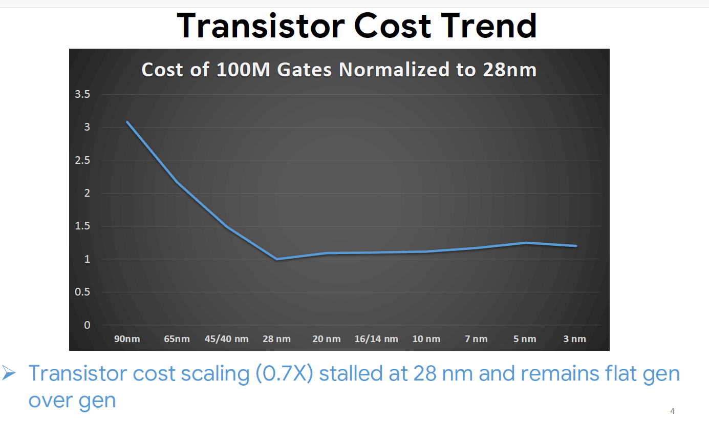
Zvi Or-Bach, chief executive of MonolithIC 3D, a 3D semiconductor integration company, presented an analysis back in 2014 that shows that per-transistor cost has stopped decreasing at 28nm. Recently, this finding was corroborated by Milind Shah from Google, who demonstrated that the per-transistor cost for 100 million gates had actually increased since 2012 when a 28nm planar process technology was put into mass production by TSMC, reports Semiconductor Digest.
"Transistor cost scaling (0.7X) stalled at 28 nm and remains flat gen-over-gen," the Google finding shows.
The industry has been concerned about diminishing returns for per-transistor costs with new nodes for quite a while. The latest chipmaking process technologies — such as 7nm, 5nm, and 3nm — require more sophisticated fab tools that cost hundreds of millions (how about $200 million in the case of an ASML Twinscan NXE litho machine?), which brings the cost of leading-edge fabs to levels from $20 billion to $30 billion. This, of course, makes production at leading-edge nodes very expensive. However, while chipmaking has gotten more complex and expensive over the years, it makes sense to take a look at the bigger picture here.
Indeed, based on the graph presented by Milind Shah from Google at the industry tradeshow IEDM, the cost of 100 million transistors normalized to 28nm is actually flat or even increasing. This lack of cost scaling makes it less appealing for some chip designs to adopt some of the latest nodes. Furthermore, it makes it more appealing to disaggregate some designs, i.e., chop them up into chiplets, instead of producing monolithic designs crafted of a single piece of silicon using a leading-edge node to optimize costs and performance.
AMD's Ryzen desktop CPUs and Intel's Meteor Lake laptop CPUs are the most obvious example of disaggregated designs in client computing space, which consist of three or four chiplets made on different process technologies at different factories. In the data center realm, AMD's epically successful EPYC data center CPUs serve as another example. Multi-billion companies like AMD and Intel can certainly assess their design options carefully and then build products using the best technologies in their possession. For smaller makers, things may not be that easy.
First up, multi-chiplet designs tend to be more power-hungry than monolithic designs, so they aren't exactly the best choice for mobile devices. Secondly, multi-chiplet integration is a tough engineering task, and while companies like MonolithIC 3D offer their multi-chiplet integration services (ultimately using advanced packaging technologies, such as Intel's Foveros or TSMC's CoWoS), their services cost money. Thirdly, advanced packaging technologies are expensive, and getting CoWoS allocation is as hard as getting a leading-edge node allocation.
To that end, while new nodes may no longer make transistors cheaper, they still make a lot of sense for many designs that either cannot be disaggregated efficiently or are hard to disaggregate due to complications with their manufacturing.
Get Tom's Hardware's best news and in-depth reviews, straight to your inbox.

Anton Shilov is a contributing writer at Tom’s Hardware. Over the past couple of decades, he has covered everything from CPUs and GPUs to supercomputers and from modern process technologies and latest fab tools to high-tech industry trends.
-
edzieba This is not 'new' news, it has been known for the last decade too. When the gate oxide thickness limit was reached ~22nm, it meant transistor scale basically remained fixed since then (barring geometry changes like GAA) and voltage scaling also ceased (why chips have been at ~1v for a decade). It's the main factor behind why for chips where performance scales closely with transistor count that those same designs have been reaching a price/performance asymptote.Reply -
bit_user It's nice to see this issue get more publicity. I've picked up on it since the current pricing trends in GPUs became a topic of controversy. Here are a few more key details I've found.Reply
Why is that happening? Let's start by looking at wafer price trends:
So, should we blame TSMC or ASML for being greedy?
Maybe not. Newer wafers are objectively more resource-intensive to produce.
Furthermore, design costs are also increasing at a similar pace:
It makes sense that dies with exponentially more components would take longer to design & test, especially to the extent that humans remain in the loop.
while new nodes may no longer make transistors cheaper, they still make a lot of sense for many designs that either cannot be disaggregated efficiently or are hard to disaggregate due to complications with their manufacturing.
And let's not forget performance (and its sister, efficiency)! Newer nodes are nearly always more efficient (e.g. offering more performance at the same power; or less power at the same performance). That's why cutting edge designs will always prefer newer nodes for logic, which still exhibits good scaling.
A big argument for chiplets is that SRAM and I/O don't scale as well as logic. So, if the benefits of a newer node are less (or even negligible), then why pay the higher price? Putting them on a separate die enables cost savings. If you're already doing a multi-die design for yield reasons, this becomes a very easy decision. -
bit_user Reply
The article says as much, in the very first sentence.edzieba said:This is not 'new' news, it has been known for the last decade too.
Wasn't fin FET also intended to work around that?edzieba said:When the gate oxide thickness limit was reached ~22nm, it meant transistor scale basically remained fixed since then (barring geometry changes like GAA)
Your reasoning is too simplistic. Essentially, you're claiming that transistor scaling stopped, yet it hasn't.edzieba said:It's the main factor behind why for chips where performance scales closely with transistor count that those same designs have been reaching a price/performance asymptote.
I think the main story is that wafer costs have increased at a similar rate as density, because it's become more complex and required more expensive equipment to push density ever higher.
A side-story is that density improvements have plateaued for things like I/O and SRAM. However, it does appear still to be ongoing, for logic. -
Co BIY Also explains clearly why TSMC is still building capacity (And consolidating older customers) at 28nm and others like Global Foundries stopped investing in advanced nodes at around the same size. It's a sweet spot in a mature industry at that point.Reply -
bit_user Reply
Back in 2019, Eben Upton said, in an interview on this site, that the Raspberry Pi was likely to stay at 28 nm, since that's where the lowest cost per transistor was (and didn't appear likely to change, in the near future).Co BIY said:Also explains clearly why TSMC is still building capacity (And consolidating older customers) at 28nm and others like Global Foundries stopped investing in advanced nodes at around the same size. It's a sweet spot in a mature industry at that point.
"28nm brings quite substantial improvements in energy. It's also the current "value node" (lowest cost per transistor), and I think will remain so for the foreseeable future."
https://forums.tomshardware.com/threads/raspberry-pi-ama-ask-your-questions-now.3492239/post-21119030(Eben Upton, June 27, 2019)
I was therefore a bit surprised that the Pi v5 seems to have moved to a smaller node, but I guess they decided the market demands for more performance were sufficient to justify a higher price. -
Paul Alcorn Here's a fun throwback; Lisa Su pointed this out back in 2013 with a chart:Reply
https://www.design-reuse.com/articles/36150/moore-s-law-is-dead-long-live-soc-designers.html
and again in 2020 at Hot Chips. -
bit_user Reply
Well spotted!PaulAlcorn said:Here's a fun throwback; Lisa Su pointed this out back in 2013 with a chart:
https://www.design-reuse.com/articles/36150/moore-s-law-is-dead-long-live-soc-designers.html
and again in 2020 at Hot Chips.
Perhaps this is one of those things the semiconductor industry almost considered common knowledge, these days. Us outsiders are only now beginning to take notice, as we start to see those semiconductors price trends having a meaningful impact on product pricing.
It does put Intel's E-core & AMD's C-core strategy in an interesting light. If transistor costs aren't going down, then you'd expect to see greater emphasis on "area-efficiency", in new designs. As long as they can increase performance per mm^2, they can increase core count and thereby perf/$ can continue to scale faster than the efficiency gains of new process nodes.
P.S. I think this article deserves to be featured in one of the panels on the front page, no?
P.P.S. Go Chiefs!!!
: ) -
refillable This analysis is too overrated, too simplistic. GM200 had almost ten times less transistors than AD102, yet the 980 Ti didn't launch anywhere near 300 USD. People think "5nm chips" are just a bunch of 5nm class transistors packed around a die. No they're not.Reply -
bit_user Reply
They didn't say anything about end product prices, did they? It was just an analysis of manufacturing costs. A lot else goes into a graphics card and its price, including software (i.e. drivers).refillable said:This analysis is too overrated, too simplistic. GM200 had almost ten times less transistors than AD102, yet the 980 Ti didn't launch anywhere near 300 USD.
I think that explains why we didn't feel the impact of higher silicon pricing until more recently. In those days, the actual GPU chip cost was probably a much smaller proportion of the total cost of a graphics card. -
refillable You have to have some degree of specificity, you can't analyze "manufacturing costs" and proceed to conclude that "transistor costs stopped going down at 28nm". It's too blanket. What are they specifically talking about? The node? What is a "node", precisely? The whole IC? Those are made up of an assortment of different transistors!Reply
It's also a moving target due to node maturity. 28 nm in its introduction (2011) had huge capacity and yield problems, making it not any cheaper than 5 nm now per die size (GK104, 2012, 294 mm^2 was $668, adjusted for inflation). Sound's familiar? Yes, that's the 4070 Ti and the 4070 super (AD104).
bit_user said:They didn't say anything about end product prices, did they? It was just an analysis of manufacturing costs. A lot else goes into a graphics card and its price, including software (i.e. drivers).
I think that explains why we didn't feel the impact of higher silicon pricing until more recently. In those days, the actual GPU chip cost was probably a much smaller proportion of the total cost of a graphics card.
There's a reason why I didn't say exactly 90% less (that'd be 159.99), or 124 USD, adjusted for inflation.
If you want a more representative example, take a look at 2700K vs 14700K. Former had a 450 USD (adjusted) MSRP, 995M transistors, fabbed on 32 nm while latter has a 420 USD MSRP and 14B transistors (estimated). 28 nm was considered the "half shrink" of 32. "Transistors became 15 times cheaper", no?
Go back 4 nodes from 32, you have Northwood at 130 nm. It was released at ~500 USD (adjusted, prices hard to track) and had 55M transistors. "Transistors had became 20 times cheaper", this time yes?
Wait what?
