Researchers developing next generation 2D semiconductors investigate potential silicon replacement in transition-metal dichalcogenide
The next-generation of chip material could be so thin to be just as three atoms thick.

Researchers at the U.S Department of Energy’s Princeton Plasma Physics Laboratory (PPPL) are developing the next generation of chips that will be smaller, thinner, and more efficient. The research team, led by Shoaib Khalid, is investigating the use of transition-metal dichalcogenide (TMD) to replace silicon in processors.
In an interview with Tom’s Hardware, Shoaib said, “The chips are getting smaller and smaller, such that their limit is almost reached in terms of functionality and size.” Moore’s Law states that the count of transistors in semiconductors will double every two years. However, as the process nodes become smaller, Moore’s Law is expected to slow down to three years, instead of the usual two. After that, we will soon reach the physical limits of semiconductors as we start hitting the two-nanometer scale or smaller.
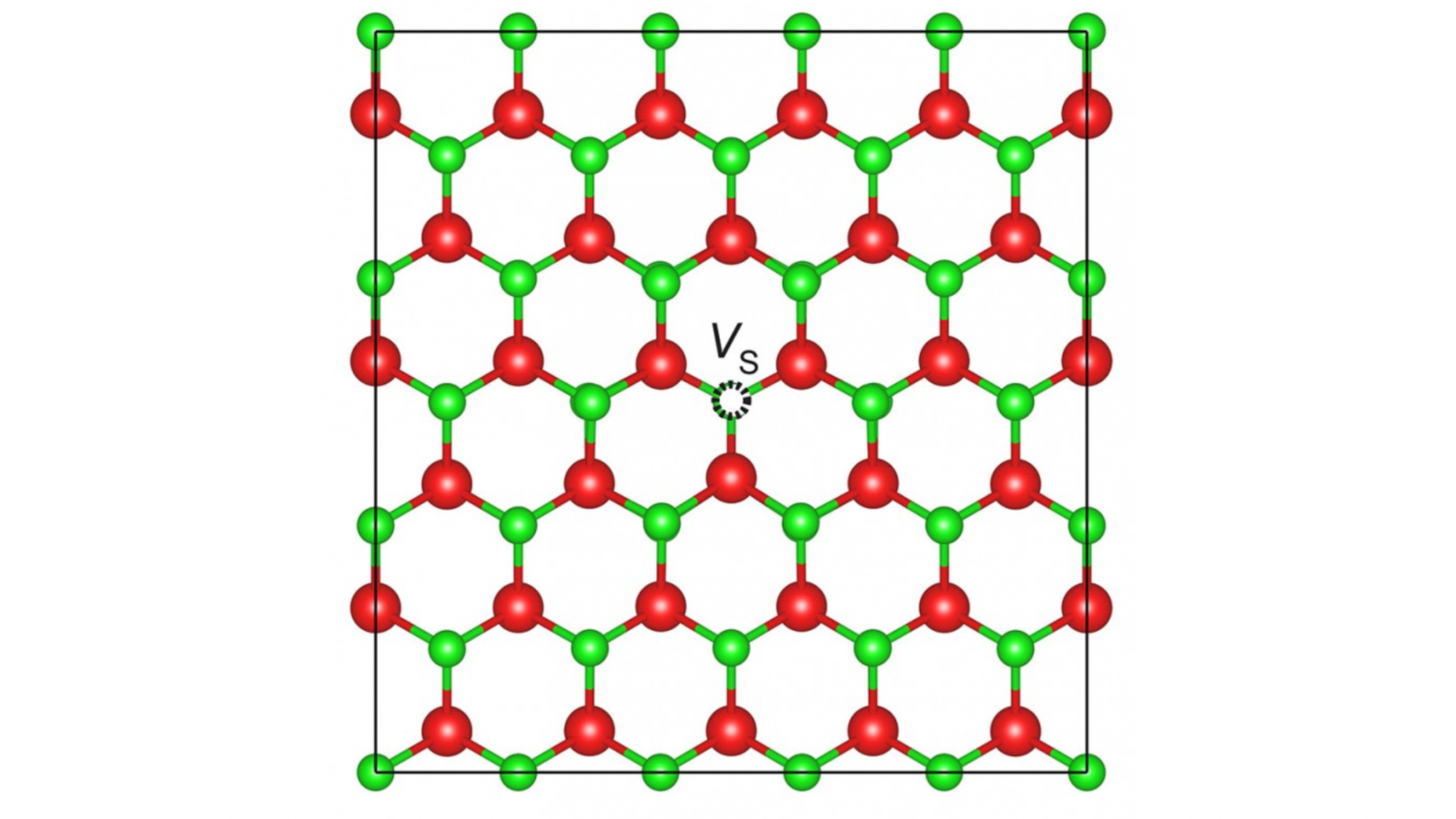
Shoaib and his team are investigating the use of TMD as a 2D material to replace the current 3D chip design. TMDs can be as thin as three atoms and act like a metal sandwich — the ‘bread’ uses chalcogen elements, also known as elements from the oxygen family. This could either by oxygen, sulfur, selenium, or tellurium. Any transition metal can then serve as filling for the ‘sandwich’.
Since TMDs are so thin, tiny alterations, such as a missing or extra atom in any layer, would impact the material’s performance. Although these alterations are called ‘defects’, they are not necessarily an unwanted phenomenon. For example, the presence of hydrogen during the TMD’s manufacturing process causes an excess of electrons. This gives the TMD a negative charge.

Shoaib said, “Depending on the type and nature of defects, they behave differently in a material and can change the properties of the material. For example, they can create excess electrons in the material, making it n-type (material with more electrons) or create more holes, making it p-type (material with more holes or positive charge).”
Computer chips use a combination of negatively charged (n-type) and positively charge (p-type) material to deliver better electrical conductivity. Current semiconductor technology uses doping to get these properties on purpose. By knowing how defects on TMDs are induced, we can then create these n-type and p-type material, but on the atomic scale.
The principles behind silicon semiconductors and TMDs are the same, but the latter have several advantages. Shoaib says that TMDs have tunable bandgaps controlled by changing the number of layers; they can be as thin as a monolayer, which is just three atoms high. You can use different materials to create them and they are flexible but durable. “In the end, the goal is to have smarter and cheaper chips,” say Shoaib.
Get Tom's Hardware's best news and in-depth reviews, straight to your inbox.
The problems that Shoaib and his team are tackling today are likely the same ones that the researchers working on the first semiconductors were facing 50 years ago. However, they were working at a bigger scale, size-wise. The PPPL team is solving the same issue, but at an atomic level.
So, how soon will we see TMDs inside our phones and PCs? TSMC is already looking at 1nm chips, with other companies introducing a roadmap to sub-nanometer transistors by 2036. “Companies like Intel are already working on making transistors from these TMDs,” says Shoaib. “I think, by 2030, we might have an actual TMD transistor that can be used in devices.”

Jowi Morales is a tech enthusiast with years of experience working in the industry. He’s been writing with several tech publications since 2021, where he’s been interested in tech hardware and consumer electronics.
-
edzieba A Chaclogenide-based IC technology has already been and gone at mass production scale: 3D XPoint.Reply -
DougMcC Given how rapidly we are closing in on monoatomic patterning, this won't make much difference to Moore's law. We'll get one, maybe two extra generations out of it at most. We really need people thinking about what comes next. How do we build subatomic computers, or 3d computing structures at building scale that don't require nuclear plants to power?Reply