Imec, the world's most advanced semiconductor research firm, recently shared its sub-1nm silicon and transistor roadmap at its ITF World event in Antwerp, Belgium. The roadmap gives us an idea of the timelines through 2036 for the next major process nodes and transistor architectures the company will research and develop in its labs in cooperation with industry giants, such as TSMC, Intel, Nvidia, AMD, Samsung, and ASML, among many others. The company also outlined a shift to what it dubs CMOS 2.0, which will involve breaking down the functional units of a chip, like L1 and L2 caches, into 3D designs that are more advanced than today's chiplet-based approaches.
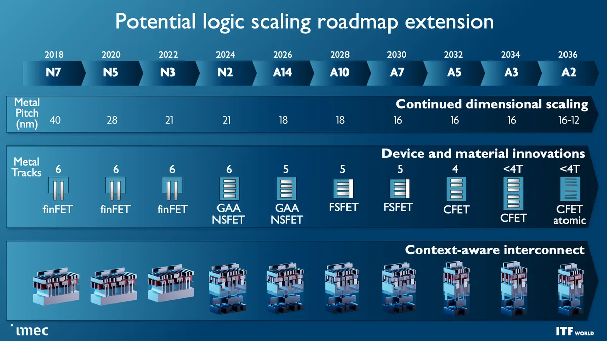
As a reminder, ten Angstroms equal 1nm, so Imec's roadmap encompasses sub-'1nm' process nodes. The roadmap outlines that standard FinFET transistors will last until 3nm but then transition to the new Gate All Around (GAA) nanosheet designs that will enter high-volume production in 2024. Imec charts the course to forksheet designs at 2nm and A7 (0.7nm), respectively, followed by breakthrough designs like CFETs and atomic channels at A5 and A2.
Moving to these smaller nodes is becoming more expensive over time, and the standard approach of building monolithic chips with a single large die has already given way to chiplets. Chiplet-based designs break various chip functions into distinct dies connected together, thus allowing the chip to function as one cohesive unit — albeit with tradeoffs.
Imec's vision of the CMOS 2.0 paradigm includes breaking the chips into even smaller pieces, with caches and memories split into their own units with different transistors, then stacked in a 3D arrangement atop the other chip functions. This methodology will also lean heavily on backside power delivery networks (BPDN) that route all power through the backside of the transistor.
Let's take a closer look at the imec roadmap and the new CMOS 2.0 methodology.


As you can see in the album above, the industry faces seemingly insurmountable challenges as nodes progress, yet the demand for more computing power, particularly for machine learning and AI, has increased exponentially. That demand hasn't been easy to satisfy; costs have skyrocketed while power consumption has steadily increased with high-end chips — power scaling remains a challenge as CMOS operating voltages have stubbornly refused to drop below 0.7 volts, and the continued need to scale to larger chips presents power and cooling challenges that will require entirely new solutions to circumvent.
And while transistor counts continue to double on a predictable Moore's Law path, other foundational issues are also becoming increasingly problematic with each new generation of chips, like the limitations of interconnect bandwidth that has severely lagged the computational capabilities of modern CPUs and GPUs, thus hampering performance and limiting the effectiveness of those extra transistors.
The imec Transistor and Process Node Roadmap


Faster and denser transistors are the first priority, though, and the first wave of those transistors will come with the Gate All Around (GAA)/Nanosheet devices that debut in 2024 with the 2nm node, replacing the triple-gate FinFETs that power today's leading-edge chips. GAA transistors confer transistor density and performance improvements, like faster transistor switching while using the same drive current as multiple fins. Leakage is also significantly reduced because the channels are surrounded entirely by a gate, and adjusting the thickness of the channel can optimize for either power consumption or performance.
We've already seen several chipmakers embrace different variations of this transistor technology. Industry leader TSMC plans for its N2 node with GAA to arrive in 2025, so it will be the last to adopt the new type of transistor. Intel's quad-sheet RibbonFET with the 'Intel 20A' process node features four stacked nanosheets, each surrounded entirely by a gate, and will debut in 2024. Samsung was the first to produce GAA for shipping products, but the low-volume SF3E pipe-cleaner node won't see mass production. Instead, the company will debut its advanced node for high volume manufacturing in 2024.
As a reminder, ten Angstroms (A) equal one 1nm. That means A14 is 1.4nm, A10 is 1nm, and we go to the sub-1nm era in the 2030 timeframe with A7. Remember that these metrics often don't match the actual physical dimensions on the chip, though.
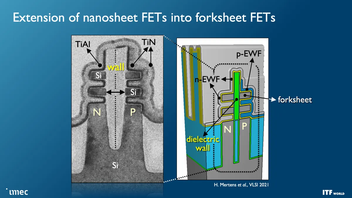
Imec expects forksheet transistors to begin at 1nm (A10) and last through the A7 node (0.7nm). As you can see in the second slide, this design stacks the NMOS and PMOS separately yet partitions them with a dielectric barrier, allowing for more performance and/or better density.
Complementary FET (CFET) transistors will shrink the footprint even further when they first arrive with the 1nm node (A10) in 2028, allowing more densely-packed standard cell libraries. Eventually, we'll see versions of CFET with atomic channels, further improving performance and scalability. CFET transistors, which you can read more about here, stack N- and PMOS devices atop each other to enable higher density. CFET should mark the end of scaling for nanosheet devices, and the end of the visible roadmap.
However, other important techniques will be needed to break the performance, power, and density scaling barriers, which imec envisions will require a new CMOS 2.0 paradigm and system technology co-optimization (SCTO).
STCO and Backside Power Delivery


At the highest level, system technology co-optimization (STCO) requires rethinking the design process by modeling the needs of the system and the target applications and then using that knowledge to inform the design decisions that go into creating the chip. This design methodology often results in 'disintegrating' the functional units typically found as part of a monolithic processor, like power delivery, I/O, and cache, and splitting them into separate units to optimize each unit for the required performance characteristics by using different types of transistors, with then also improves the cost.
One of the goals of fully disaggregating the standard chip design is to split out caches/memory to their own distinct layer of a 3D-stacked design (more on this below), but this requires reducing the complexity at the top of the chip stack. Revamping the Back End of Line (BEOL) processes, which focus on wiring the transistors together and enabling both communication (signals) and power delivery, is key to this effort.
Unlike today's designs that deliver power from the top of the chip down to the transistors, backside power distribution networks (BPDN) route all power directly to the backside of the transistor with TSVs, thus separating power delivery from the data transmission interconnects that remain in their normal location on the other side. Separating the power circuitry and the data-carrying interconnects improves voltage droop characteristics, allowing for faster transistor switching while enabling denser signal routing on the top of the chip. Signal integrity also benefits because the simplified routing enables faster wires with reduced resistance and capacitance.
Moving the power delivery network to the bottom of the chip enables easier wafer-to-wafer bonding at the top of the die, thus unlocking the potential to stack logic on memory. Imec even envisions possibly moving other functions to the backside of the wafer, like the global interconnect or clock signals.
Intel has already announced its own version of the BPDN technique, dubbed PowerVIA, that will debut in 2024 with the 20A node. Intel is set to reveal more details about this technology at the upcoming VLSI event. Meanwhile, TSMC has also announced that it will bring BPDN to its N2P node that will be in high-volume production in 2026, so it will lag Intel for quite some time with this tech. Samsung is also rumored to adopt this tech with its 2nm node.
CMOS 2.0: The Path to Truly 3D Chips


CMOS 2.0 is the culmination of imec's vision for future chip designs, encompassing fully 3D chip designs. We're already seen memory stacking with AMD's second-gen 3D V-Cache that stacks L3 memory atop the processor to boost memory capacity, but imec envisions the entire cache hierarchy being contained in its own layers, with L1, L2, and L3 caches being vertically stacked on their own dies above the transistors that comprise the processing cores.
Each level of cache would be created with the transistors best suited for the task, meaning older nodes for SRAM, which is becoming more important as SRAM scaling has begun to slow tremendously. SRAM's reduced scaling has led to caches consuming a higher percentage of the die, thus leading to increased cost-per-MB and disincentivizing chipmakers from using larger caches. As such, the cost reductions associated with moving to less-dense nodes for cache with 3D stacking could also lead to much larger caches than we've seen in the past. If implemented correctly, 3D stacking can also help alleviate latency concerns associated with larger caches.
These CMOS 2.0 techniques will leverage 3D stacking technology, like wafer-to-wafer hybrid bonding, to form a direct die-to-die 3D interconnect, which you can read more about here.
As you can see in the above album, Imec also has a 3D-SOC roadmap that outlines continued shrinking for the interconnects that will tie together the 3D designs, thus enabling faster and denser interconnects in the future. These advances will be realized by using newer types of interconnects and processing methods in the coming years.
About imec
You might not be familiar with the Interuniversity Microelectronics Centre (imec), but it ranks among the most important companies in the world. Think of imec as a silicon Switzerland, of sorts. Imec serves as a quiet cornerstone of the industry, bringing fierce rivals like AMD, Intel, Nvidia, TSMC, and Samsung together with chip toolmakers such as ASML and Applied Materials, not to mention the critical semiconductor software design companies (EDA) like Cadence and Synopsys, among others, in a non-competitive environment.
This collaboration allows the companies to work together to define the roadmap of the next generation of tools and software they will use to design and manufacture the chips that power the world. A standardized approach is paramount in the face of the profoundly increasing cost and complexity of the chipmaking process. The leading-edge chipmakers use much of the same equipment sourced from a few critical toolmakers, so some level of standardization is necessary, and circumventing the laws of physics requires R&D efforts that can begin a decade in advance, so imec’s roadmaps give us a broad view of the upcoming advances in the semiconductor industry.
