Nvidia outlines plans for using light for communication between AI GPUs by 2026 — silicon photonics and co-packaged optics may become mandatory for next-gen AI data centers
Nvidia's CPO enables faster connections at lower power.

Get Tom's Hardware's best news and in-depth reviews, straight to your inbox.
You are now subscribed
Your newsletter sign-up was successful
The extreme demands of passing communication between ever-growing clusters of AI GPUs is fueling a move towards using light for communication across the networking layers. Earlier this year, Nvidia outlined that its next-generation rack-scale AI platforms will use silicon photonics interconnects with co-packaged optics (CPO) for higher transfer rates at lower power. At the Hot Chips conference this year, Nvidia released some additional information about its next-generation Quantum-X and Spectrum-X photonics interconnection solutions and when they will arrive in 2026.
Nvidia's roadmap will likely closely follow TSMC's COUPE roadmap, which unfolds in three stages. The first generation is an optical engine for OSFP connectors, offering 1.6 Tb/s data transfer while reducing power consumption. The second generation moves into CoWoS packaging with co-packaged optics, enabling 6.4 Tb/s at the motherboard level. The third generation aims for 12.8 Tb/s within processor packages and targets further cuts in power and latency.
Why CPO?
In large-scale AI clusters, thousands of GPUs must behave as one system, which introduces challenges in how these processors must be interconnected: instead of each rack having its own Tier-1 (Top-of-Rack) switch linked by short copper cables, the switches are moved to the end of the row to create a consistent, low-latency fabric across multiple racks. This relocation greatly extends the distance between servers and their first switch, which makes copper impractical at speeds like 800 Gb/s, so optical connections are required for nearly every server-to-switch and switch-to-switch link.
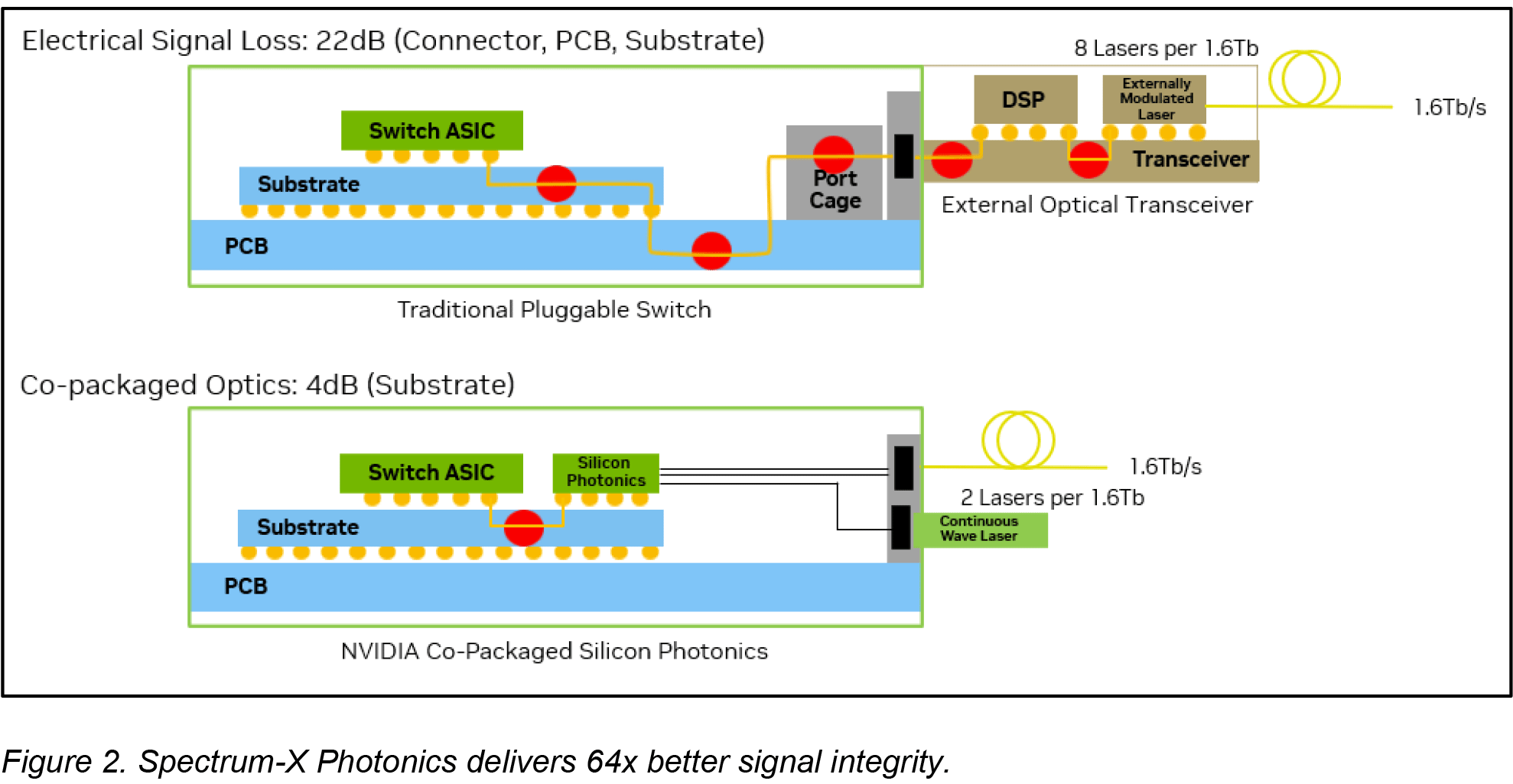
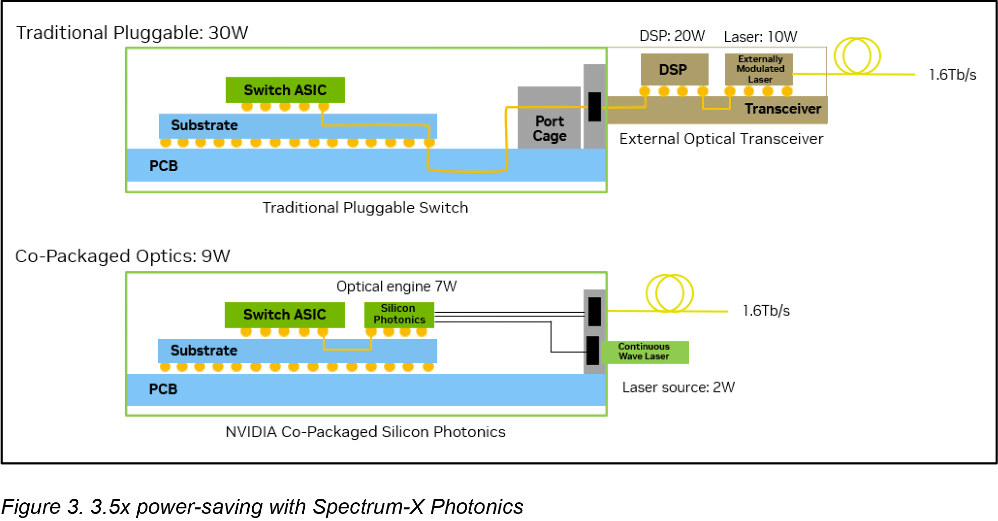
Article continues belowUsing pluggable optical modules in this environment introduces clear limits: data signals in such designs leave the ASIC, travel across the board and connectors, and only then are converted to light. That method produces severe electrical loss, up to roughly 22 decibels on 200 Gb/s channels, which requires compensation that uses complex processing and increases per-port power consumption to 30W (which in turn calls for additional cooling and creates a point of potential failure), which becomes almost unbearable as the scale of AI deployments grow, according to Nvidia.
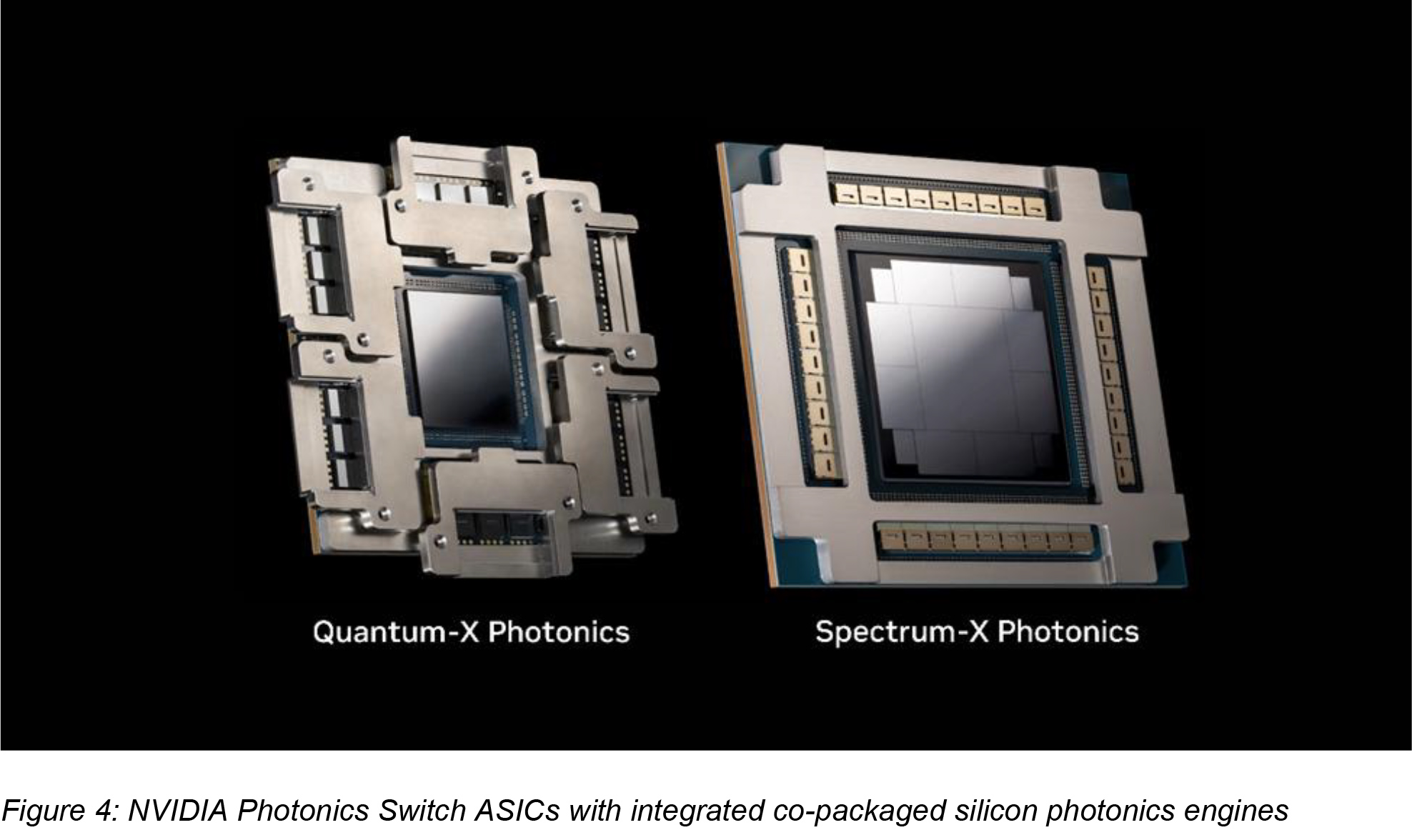
CPO sidesteps penalties of traditional pluggable optical modules by embedding the optical conversion engine alongside the switch ASIC, so instead of traveling over long electrical traces, the signal is coupled to fiber almost immediately. As a result, electrical loss is cut to 4 decibels, and per-port power consumption is reduced to 9W. Such a layout removes numerous components that could fail and greatly simplifies the implementation of optical interconnects.
Nvidia claims that by moving away from traditional pluggable transceivers and integrating optical engines directly into switch silicon (courtesy of TSMC’s COUPE platform), it achieves very substantial gains in efficiency, reliability, and scalability. Improvements of CPOs compared to pluggable modules are dramatic, according to Nvidia: a 3.5-times increase in power efficiency, a 64 times better signal integrity, 10 times boost in resiliency due to fewer active devices, and roughly 30% faster deployment because service and assembly are simpler.
CPOs for Ethernet and InfiniBand
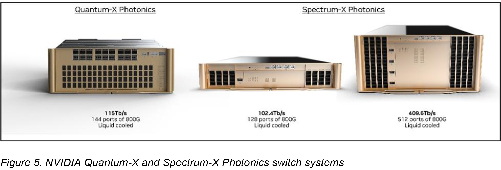
Nvidia will introduce CPO-based optical interconnection platforms both for Ethernet and InfiniBand technologies. First, the company plans to introduce Quantum-X InfiniBand switches in early 2026. Each switch will deliver 115 Tb/s of throughput, supporting 144 ports operating at 800 Gb/s each. The system also integrates an ASIC featuring 14.4 TFLOPS of in-network processing and supporting Nvidia's 4th Generation Scalable Hierarchical Aggregation Reduction Protocol (SHARP) to cut latency for collective operations. The switches will be liquid-cooled.
Get Tom's Hardware's best news and in-depth reviews, straight to your inbox.
In parallel, Nvidia is set to bring CPO into Ethernet with its Spectrum-X Photonics platform in the second half of 2026. This one will rely on the Spectrum-6 ASIC that will power two devices: the SN6810 that provides 102.4 Tb/s of bandwidth with 128 ports at 800 Gb/s, and the larger SN6800 that scales to 409.6 Tb/s and 512 ports at the same rate. Both also use liquid cooling.
Nvidia envisions that its CPO-based switches will power new AI clusters for generative AI applications that are getting larger and more sophisticated. Due to the usage of CPO, such clusters will eliminate thousands of discrete components, offering faster installation, easier servicing, and reduced power consumption per connection. As a result, clusters using Quantum-X InfiniBand and Spectrum-X Photonics offer improvements when it comes to such metrics as time-to-turn-on, time-to-first-token, and long-term reliability.
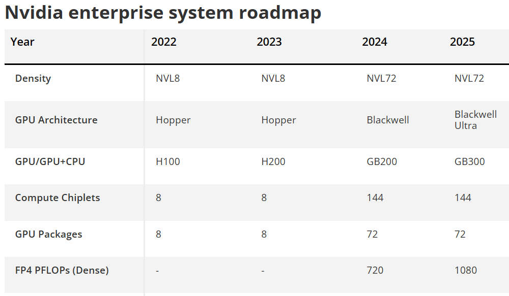
Want more? We've got an exclusive roadmap to Nvidia's enterprise GPUs and CPUs — only for subscribers of Tom's Hardware Premium.
Nvidia stresses that co-packaged optics are not an optional enhancement but a structural requirement for future AI data centers, which implies that the company will position its optical interconnects as some of the key advantages over rack-scale AI solutions from rivals, such as AMD. Which is, of course, why AMD has acquired Enosemi.
The road ahead
One important thing to note about Nvidia's silicon photonics initiative is that its evolution is tightly aligned with the evolution of TSMC's COUPE (Compact Universal Photonic Engine) platform, which is set to evolve in the coming years, thus improving Nvidia's CPO platforms too. TSMC's 1st Gen COUPE is built by stacking a 65nm electronic integrated circuit (EIC) with a photonic integrated circuit (PIC) using the company's SoIC-X packaging technology.
TSMC's COUPE roadmap unfolds in three stages. The first generation is an optical engine for OSFP connectors, offering 1.6 Tb/s data transfer while reducing power consumption. The second generation moves into CoWoS packaging with co-packaged optics, enabling 6.4 Tb/s at the motherboard level. The third generation aims for 12.8 Tb/s within processor packages and targets further cuts in power and latency.
Follow Tom's Hardware on Google News to get our up-to-date news, analysis, and reviews in your feeds. Make sure to click the Follow button.

Anton Shilov is a contributing writer at Tom’s Hardware. Over the past couple of decades, he has covered everything from CPUs and GPUs to supercomputers and from modern process technologies and latest fab tools to high-tech industry trends.
-
thisisaname Reply
Yes he did https://wccftech.com/nvidia-ceo-jensen-huang-claims-silicon-photonics-packaging-is-still-years-away/Pierce2623 said:Didn’t Jensen JUST say silicon photonics were years away from being decent? -
bwana With those guys, it’s all about distracting your competitors. Reminds me of musk warning about the existential threat of AI a couple of years ago and calling for a moratorium. Meanwhile , he was building grokReply -
Pierce2623 Reply
Thanks. I thought so.thisisaname said:Yes he did https://wccftech.com/nvidia-ceo-jensen-huang-claims-silicon-photonics-packaging-is-still-years-away/
