TSMC shares deep-dive details about its cutting edge 2nm process node at IEDM 2024 — 35 percent less power or 15 percent more performance
All the secrets revealed?

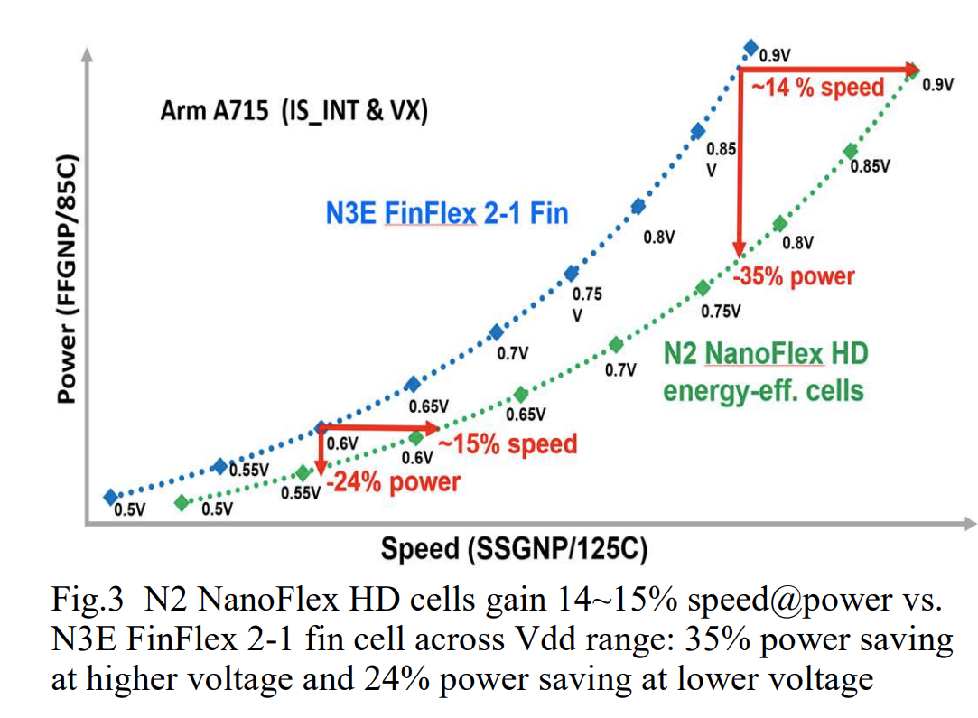
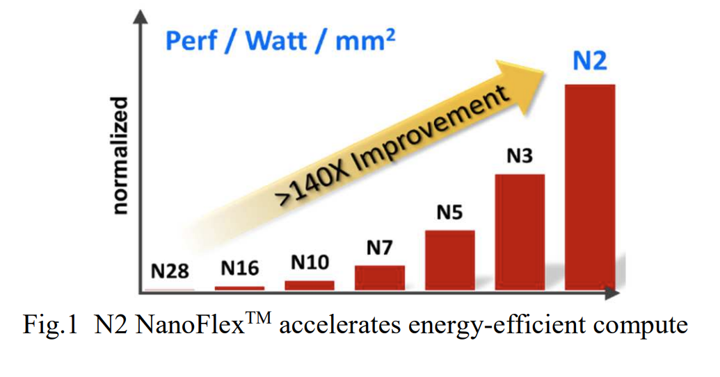
TSMC revealed additional details about its N2 (2nm-class) fabrication process at the IEEE International Electron Device Meeting (IEDM) earlier this month. The new production node promises a 24 to 35% power reduction or 15% performance improvement at the same voltage, and 1.15X higher transistor density than the prior-gen 3nm process. The vast majority of these advantages are enabled by TSMC's new gate-all-around (GAA) nanosheet transistors along with N2 NanoFlex design-technology co-optimization capability and some other enhancements detailed at IEDM.
Gate-all-around nanosheet transistors allow designers to adjust their channel width to balance performance and power efficiency. On top of that, TSMC's N2 adds N2 NanoFlex DTCO, enabling designers to develop short cells with minimum area and enhanced power efficiency, or tall cells optimized for maximum performance. The technology also includes six voltage threshold levels (6-Vt) spanning a 200mV range, achieved using TSMC's third-generation dipole-based integration with both n-type and p-type dipoles.


N2's innovations introduced at the process and device levels target not only boosting transistor drive currents by refining sheet thickness, junctions, dopant activation, and stress engineering but also reducing effective capacitance (Ceff) to achieve class-leading energy efficiency. Collectively, these refinements yield I/CV speed gains of about 70% and 110% for N-type and P-type nanosheet transistors, respectively.
Compared to FinFETs, N2 nanosheet transistors deliver noticeably better performance per watt at low supply voltage ranges of 0.5V to 0.6V, where process and device optimizations boost clocks by around 20% and cut standby power consumption by about 75% at 0.5V operation. Moreover, integrating N2 NanoFlex and multiple threshold voltage (multi-Vt) options enables additional design flexibility for energy-efficient processors at high logic densities.
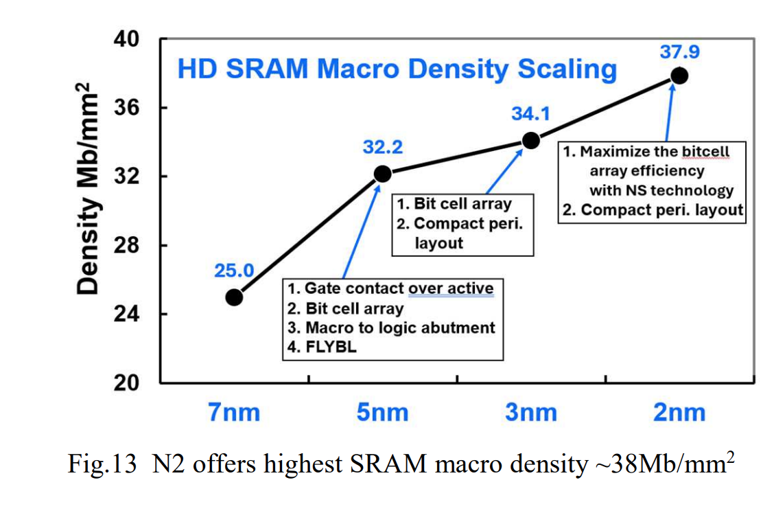
Transistor architecture and DTCO advantages directly affect SRAM scalability, which was tough to achieve with leading-edge nodes in recent years. With N2, TSMC has managed to achieve a record 2nm SRAM density of about 38Mb/mm^2. In addition to hitting record SRAM density, TSMC also lowered its power consumption. As GAA nanosheet transistors feature tighter threshold voltage variation (Vt-sigma), N2 achieves about a 20mV reduction in minimum operational voltage (Vmin) for High Current (HC) macros and a 30–35mV reduction for High Density (HD) macros compared to FinFET-based designs. These improvements enable stable SRAM read and write functionality down to approximately 0.4V while maintaining robust yields and reliability.
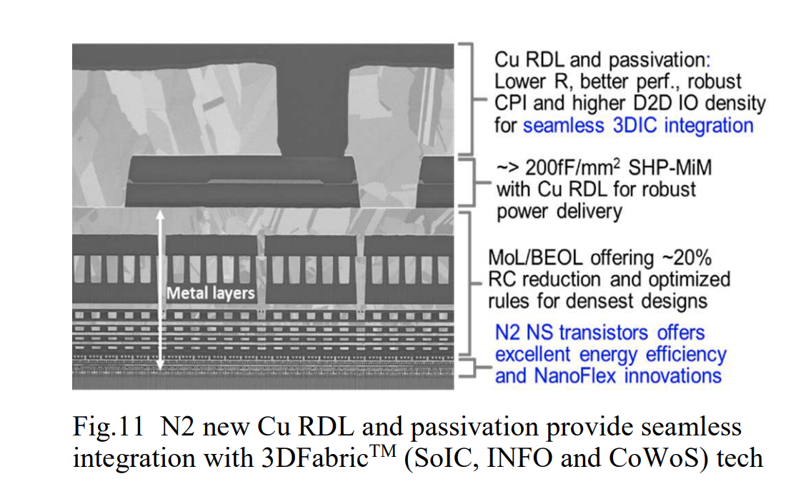
In addition to new transistors, TSMC's N2 employs all-new middle-of-line (MoL), back-end-of-line (BEOL), and far-BEOL wiring to cut resistance by 20% and improve performance efficiency. N2's MoL now uses barrier-free tungsten wiring, which reduces vertical gate contact (VG) resistance by 55% and increases the ring oscillator's frequency by about 6.2%. Additionally, the first metal layer (M1) is now created in one EUV exposure pass followed by a single etch step (1P1E), reducing complexity, lowering mask counts, and improving overall process efficiency. TSMC says that using EUV 1P1E for M1 cuts standard cell capacitance by nearly 10% and saves several EUV masks. In addition, N2 cuts metal (My) and via (Vy) resistance by 10%.
In addition, N2's extra features for HPC applications include super high-performance MiM (SHP-MiM) capacitors providing around 200fF/mm² of capacitance, which helps achieve higher maximum operating frequencies (Fmax) by reducing transient voltage droop.
Get Tom's Hardware's best news and in-depth reviews, straight to your inbox.
Finally, TSMC's N2 technology features a new Cu RDL option with flat passivation and TSVs that is optimized for face-to-face and face-to-back 3D stacking with an SoIC bond pitch of 4.5 μm, which is set to become a usable feature for AI, HPC, and even mobile designs, according to TSMC.
TSMC is set to start production on its N2 process technology in the latter half of 2025.

Anton Shilov is a contributing writer at Tom’s Hardware. Over the past couple of decades, he has covered everything from CPUs and GPUs to supercomputers and from modern process technologies and latest fab tools to high-tech industry trends.
-
Flayed Looks impressive. I wonder how many years will pass before any chips baked with this hit the consumer market.Reply -
usertests If I'm not mistaken, NanoFlex/FinFlex can allow you to have multiple types of cells on a single chip, so you could optimize for P-cores and E-cores in the same monolithic design for example.Reply
There may be no free lunch anymore but these are good efficiency gains, and SRAM scaling isn't quite dead yet.
They should appear in 2026.Flayed said:Looks impressive. I wonder how many years will pass before any chips baked with this hit the consumer market. -
bit_user I always found it a little hard to believe that backside power gives Intel such an unassailable advantage that TSMC wouldn't be able to hold court with it. I figured TSMC's N2 nodes are going to pack a lot of improvements, maybe even enough to compensate for that deficit. Perhaps we'll find out, if Intel's 18A doesn't fall too far behind schedule.Reply -
awake283 Yea, there's some smart people in this world. How is 2nm even possible! I mean, I know how they do it with lithography and EUV light and all that, but still, I dont understand how we even figured these things out in the first place. It's incredible.Reply -
Vertigo_1 Reply
The node names are not actually equivalent to the number they purport.awake283 said:Yea, there's some smart people in this world. How is 2nm even possible! I mean, I know how they do it with lithography and EUV light and all that, but still, I dont understand how we even figured these things out in the first place. It's incredible. -
usertests Reply
"2nm" is a marketing name, the names do not necessarily correlate to any feature size anymore.awake283 said:Yea, there's some smart people in this world. How is 2nm even possible! I mean, I know how they do it with lithography and EUV light and all that, but still, I dont understand how we even figured these things out in the first place. It's incredible.
There are a lot of brains in the operation though. Just look at fab tools.
https://media.wired.com/photos/6126c73a199749f5e9879dea/16:9/w_2399,h_1349,c_limit/Business-ASML---Employees-assembling-an-EUV-system-(ASML).jpg -
usertests Reply
Intel damage control is out in full force for 18A. They even got the fired CEO to defend it, incredible.bit_user said:I always found it a little hard to believe that backside power gives Intel such an unassailable advantage that TSMC wouldn't be able to hold court with it. I figured TSMC's N2 nodes are going to pack a lot of improvements, maybe even enough to compensate for that deficit. Perhaps we'll find out, if Intel's 18A doesn't fall too far behind schedule.
https://www.tomshardware.com/news/tsmc-our-3nm-node-comparable-to-intels-18nm-techhttps://www.tomshardware.com/tech-industry/intels-comeback-appears-on-track-ceo-gelsinger-says-18a-process-node-performance-is-a-little-bit-ahead-of-tsmcs-n2-but-intels-process-arrives-a-year-earlier-than-tsmcs
We've seen the backside and forth on 18A and N2. 18A's schedule will slip and won't be much better (if at all) than N2. TSMC will respond in an orderly fashion with A16 with backside power and that will be that. -
Mama Changa Reply
Not long at all: iPhone 18 in 2026 will use A20 Pro based on 2nm.Flayed said:Looks impressive. I wonder how many years will pass before any chips baked with this hit the consumer market. -
Mama Changa Reply
After Panther Lake or Nova Lake there will be no P or E cores, it will be one core that can be freely clocked to serve any role as required performance or efficiency etc.. Rentable units are coming.usertests said:If I'm not mistaken, NanoFlex/FinFlex can allow you to have multiple types of cells on a single chip, so you could optimize for P-cores and E-cores in the same monolithic design for example.
There may be no free lunch anymore but these are good efficiency gains, and SRAM scaling isn't quite dead yet.
They should appear in 2026. -
usertests Reply
I say it generally. Could apply to Intel, AMD's regular + 'C' cores, or ARM (the TSMC chart shows Cortex-A715).Mama Changa said:After Panther Lake or Nova Lake there will be no P or E cores, it will be one core that can be freely clocked to serve any role as required performance or efficiency etc.. Rentable units are coming.
Also, it should be pointed out that Intel's plans are in extreme flux, rentable units / Royal Core might not be coming, and they just ditched a CEO. Who knows what their E-core plans are anymore? Especially 3+ years out.