AMD Dishes on Zen 3 and Zen 4 Architecture, Milan and Genoa Roadmap
At the HPC-AI Advisory Council UK conference, AMD revealed new details about its Zen 3 and Zen 4 architectures, along with a roadmap that gives us the timeline and some key specs for its next-gen EPYC Milan and Genoa lines of EPYC data center chips. The presentation was uploaded to YouTube and then taken down in rather quick fashion, likely because the company wasn't ready to divulge these key details yet. We snagged a copy of the video before it was taken down and have some new details of AMD's future plans.
AMD's revolutionary Zen microarchitecture introduced the world to mass-produced chiplet-based processors that enable the company to use the same underlying design across both consumer and enterprise chips. Any changes to the company's architecture will filter out to all of its new client and enterprise chips, meaning these changes will likely come to the vaunted Ryzen lineup of chips in the future.
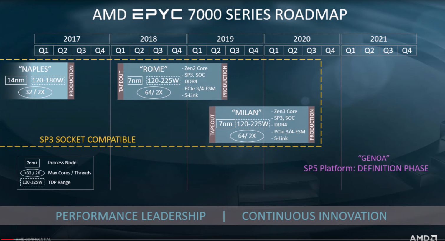
But when? AMD presented a roadmap outlining the arrival of the Milan chips, which feature Zen 3 cores, entering production in Q3 2020. That means the company is executing its plan of providing yearly updates to its architecture. The company also noted that it has already taped out the chips and is sampling them to customers.
The new Milan chips will feature the 7nm+ node, a refreshed version of the current node with higher performance. They also feature the same maximum of 64 cores as the current-gen Rome models and drop into the same SP3 socket, meaning they are backward compatible with existing platforms. They'll also come with the same support for eight channels of DDR4 and PCIe 4.0 and respect the base 120-225W TDP envelope, though it's logical to expect higher-TDP variants like the 7H12 are also in the works. The chips also have two threads per core, silencing the rather dubious rumors that AMD would switch to four threads per core (SMT4) as we see with some competing chips.
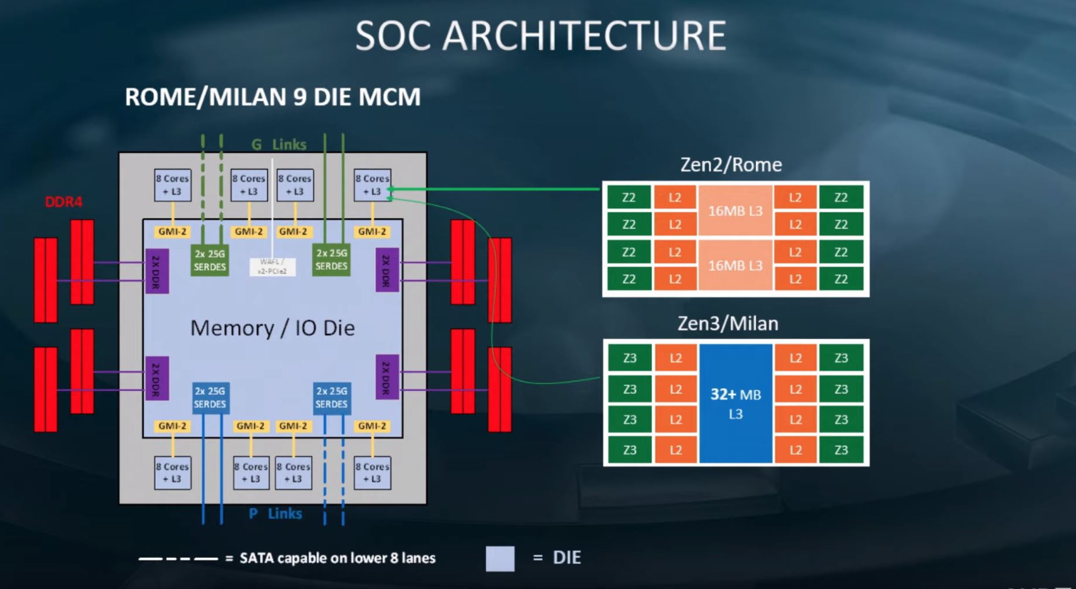
The next-gen Milan chips still feature the same nine-die arrangement as the current-gen Rome models, with eight compute die and one I/O die, along with eight cores assigned to each compute chiplet. The largely unchanged specifications, at least in key areas, implies Milan is merely a "Tock"-equivalent, or just a move to the second-gen of the 7nm node (7nm+).
However, AMD also disclosed that the company had made a significant alteration to the cache alignments inside the chip, which indicates that there is significant work being done under the hood to improve instruction per cycle (IPC) throughput and reduce latency, both of which are key focus areas for AMD as it evolves its architecture. AMD currently splits its chiplets into two four-core Compute Complexes (CCX), each armed with 16MB of L3 cache. For Milan, that changes to eight cores connected to a unified 32MB slice of L3 cache, which should eliminate a layer of latency within the compute die.
Much of the success of a design hinges on its ability to feed the execution cores with data (feeding the beast, as it were), and significance improvements in these areas will bring along an increase in IPC, giving us more performance gains than we would normally expect from a mere refresh generation. Pair that with improved frequency from a faster and more mature variant of the 7nm process and AMD could provide some exceptional gen-on-gen performance gains, regardless if core counts remain static.
Get Tom's Hardware's best news and in-depth reviews, straight to your inbox.
That feeds into AMD's assertion that it would continue to provide groundbreaking new levels of performance with each iteration of its microarchitecture, breaking the mold of incremental performance updates that we've become accustomed to during Intel's decade of dominance.
AMD continues onward with its next-next-gen Genoa architecture that is already in the "definition phase." The chip will drop into a new SP5 socket and land somewhere in the 2021 time frame. The company says Genoa will come with "new memory," likely meaning DDR5. We're sure AMD is also considering a jump to PCIe 5.0.
Intel isn't sitting idly by, though, with purported plans to be on the Sapphire Rapids chips in Q1 2021, with a rumored 8-channel DDR5 design and support for PCIe 5.0. It's clear that the two companies will continue to trade blows for years to come in an ever more competitive market.

Paul Alcorn is the Editor-in-Chief for Tom's Hardware US. He also writes news and reviews on CPUs, storage, and enterprise hardware.
-
bit_user It's so kind of them to show us when the tapeouts are. I'm surprised that even got put into a slide.Reply
For those who don't know, "tape-out" is when the design is first sent to the fab. Between that and production, you have a couple respins, with probably the later ones serving as engineering samples for board partners.
https://en.wikipedia.org/wiki/Tape-out -
Gillerer I disagree about the sweeping statement of "eliminating one layer of latency within the compute die".The only situation where that happens is if you only have one compute die (CCD), since that will then no longer have multiple CCXes, so the latency layer of inter-CCX communication is removed.Reply
If you have multiple CCDs, communication between cores on them will still make a hop by the I/O die, just as between two CCXes do on Zen 2 (even if they're physically located on the same CCD). Even though the higher latency is incurred less frequently (since there are now 7 neighboring cores instead of 3), it is by no means "eliminated".
Also, the fact that you double the L3 cache accessible to each core - and therefore less likely to have to go to system memory - doesn't remove any latency layers, just alters the chances of hitting them.The place I would anticipate the most advancement is from combining the Infinity Fabric links of two CCXes into a single link. This could give a single core double the memory and I/O throughput (to the I/O die), as long as there is little contention for the resources with other cores.
EDIT: I stand corrected. It seems I had misunderstood this - getting a couple of terms mixed - when I first read about Ryzen 3000 during launch. The text I remembered was referring to intra-package, not intra-die communication (lack of direct links between CCDs). Shouldn't read technical material quickly... -
bit_user Reply
Huh? So, even between two CCX's on the same die, you still have a round-trip to the I/O die? That kinda sucks.Gillerer said:between two CCXes do on Zen 2 (even if they're physically located on the same CCD). -
Paul Alcorn There is an infinity fabric connection between the two CCX within a single die/chiplet. Much like you see in the graphic in the link below. (The infinity symbol between these two CCX denotes that connection.) Two CCXes on a single die communicate across that fabric via this intra-die connection, essentially you have two quad-core CPUs talking to each other. The problem comes in when you have to hop to other die. https://www.tomshardware.com/reviews/amd-ccx-definition-cpu-core-explained,6338.htmlReply -
bit_user Reply
Big thanks! That seems much more energy- & latency- efficient.PaulAlcorn said:There is an infinity fabric connection between the two CCX within a single die/chiplet.
One reason I want an APU is to have only one CCX. I'm trying to get a Ryzen 5 Pro 3400G. -
hannibal Replybit_user said:Big thanks! That seems much more energy- & latency- efficient.
One reason I want an APU is to have only one CCX. I'm trying to get a Ryzen 5 Pro 3400G.
You mean ryzen 4400g... Because 3400G is old Zen+ technology aka monolith architecture. Or do you mean that you want to get both cpu and gpu in one die. Then the 3400g is way to go! Zen2 Apus comes (maybe) next year. -
bit_user Reply
Right now, I want a Ryzen 5 Pro 3400G. They were just announced. Pro version, because it's for a small file server and I want ECC memory, which the non-Pro APUs don't support.hannibal said:You mean ryzen 4400g... Because 3400G is old Zen+ technology aka monolith architecture.
The reasons I want an APU are:
cost
I only need 4 cores
1 CCX = better & more-efficient inter-core communication
avoid the need for a separate GPU - the machine mostly runs headless.
As it's replacing a Phenom II, Zen+ will be a fine upgrade.hannibal said:Zen2 Apus comes (maybe) next year. -
djayjp "The largely unchanged specifications, at least in key areas, implies Milan is merely a "Tock"-equivalent, or just a move to the second-gen of the 7nm node (7nm+)."Reply
You mean "tick": Intel's tock involved a significant microarchitectural change. -
hannibal Replybit_user said:Right now, I want a Ryzen 5 Pro 3400G. They were just announced. Pro version, because it's for a small file server and I want ECC memory, which the non-Pro APUs don't support.
As it's replacing a Phenom II, Zen+ will be a fine upgrade.
Yeah! In your cace it definily is a good choise! -
bit_user Reply
It'll be interesting to see what EUV does, for TSMC's 7 nm.djayjp said:"The largely unchanged specifications, at least in key areas, implies Milan is merely a "Tock"-equivalent, or just a move to the second-gen of the 7nm node (7nm+)."
Really? I kinda thought the whole tick-tock thing started with Sandybridge. Ivy Bridge was mostly just a node-shrink. So, then ticks should be the bigger architectural changes.djayjp said:You mean "tick": Intel's tock involved a significant microarchitectural change.
Also, people like to joke that Intel's scheme, since Skylake, has been tick-tock-tock-tock-tock...


