PrimeCables C05132 Charging Station Tear-Down: Organizational Power
DC-DC Converter
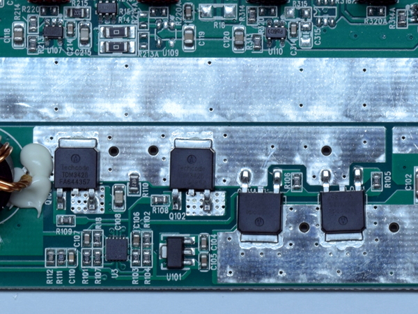
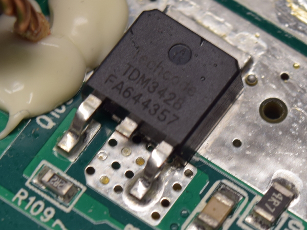
The charging station’s bulk DC-DC converter responsible for stepping 19V input down to high-current 5V output consists of four Techcode TDM3428 N-FETs (30V 40A at less than 9.8mΩ) operating as parallel pairs, another 78L05 regulator dedicated to powering the controller, the Techcode TD1730 controller itself, and its many support components.
Under the maximum load I was able to test the DC-DC converter at, its FETs were merely coffee-mug-warm. That makes sense considering how each device averages less than 7A, which should translate to less than 1W each, including switching losses. That's no challenge at all for the large tinned copper pours and bottom ground plane in open air.
Thermal Vias
Aside from coupling heat between layers by leveraging surface area, another method consists of cribbing the board with vias, plating them, and, optionally, soldering over them. You can see that a few holes did wick up some solder here.
Article continues belowHow does this work? Simple: copper and tin have much lower thermal resistance than FR4 and most other common board materials, so the vias simply give heat a lower resistance path through the board. This is especially effective when the pads are electrically connected to power or ground planes on other layers, such as the bottom’s ground plane in this instance.
DC-DC Converter Output Filter
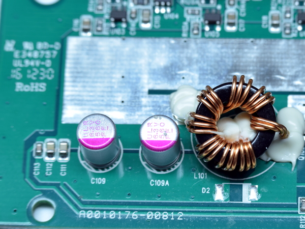
An inductor carrying current in excess of 13A at a high switching frequency requires a large conductor surface area to offset skin effect. This is commonly achieved by splitting the load across multiple smaller wires, three doing eight laps around the core in this case. A pair of what appear to be 560µF 6.3V X-Con (SamXon) ULR polymer capacitors handles bulk output filtering.
What about the ceramic capacitor trio? The smaller they are, the closer they need to be to what they're meant to filter. Their segregated location in the bottom-left corner, directly in front of the voltage feedback tap and with the smallest cap last in line, tells me that their primary purpose must be reducing the amount of noise fed into that trace.
Port Protection: Independent 2.4A Ports
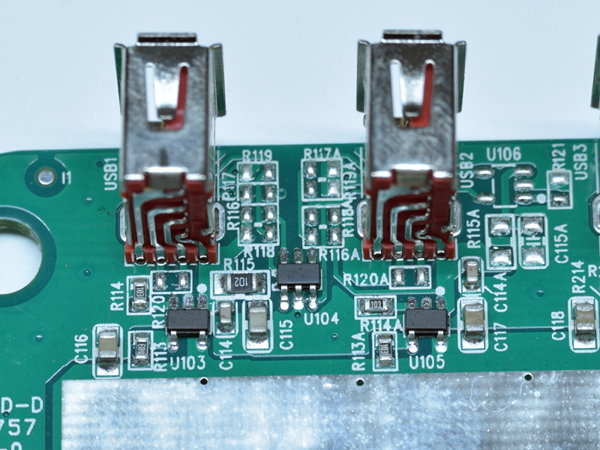
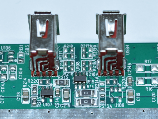
The first pair of ports features a dedicated Techcode TD9517 electronic fuse (2.5A minimum, 2.8A typical, and 3.2A maximum trip current with 62mΩ on-resistance) and related support components for each port. Between the two ports, we find unpopulated pads for resistor-based charging standard identification and the same dual-port CX2901 multi-standard charger ID chip found in Aukey’s PA-U32.
Get Tom's Hardware's best news and in-depth reviews, straight to your inbox.
In testing, these ports delivered up to 2.85A cold and 2.6A after warming up with a short-circuit.
Port Protection: Shared 2.4A Ports
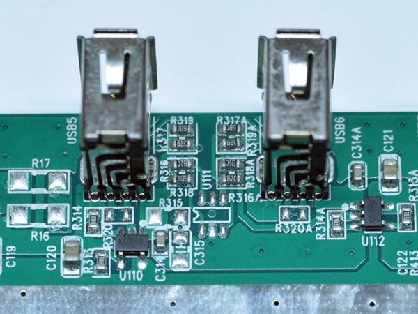
The next two ports share a single TD9517 chip on the left, which ties onto the next port to the right via two zero-ohm resistor links and a wide trace on the board’s bottom. Just like the first port pair, these two also feature unpopulated pads for resistor-based standard identification and a CX2901 chip. Apart from the jumper resistors piggy-backing the vacant right e-fuse footprint onto the left port’s, this is practically the same layout as the first port pair.
And just like the first port pair, this one's shared electronic fuse also passes 2.8A cold and 2.6A warmed up.
Port Protection: Resistor ID
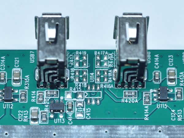
The third set of ports, which is also the first 1A pair, ditches the IC-based charging standard identification by vacating its footprint in favor of old-fashioned resistor dividers. These ports still use electronic fuses, but those are labeled Pb6D3 and I couldn't find specifications for them. For some reason, the second protection chip is rotated 90° instead of following the first five ports’ orientation. From how inconsistent routing between ports is, I’d hazard a guess that the designer placed and locked location-critical components, then let the auto-router deal with the rest.
To the left, you can also see R16 and R17 hinting that the fifth port may get ganged up with the fourth (instead of the third) on some product variants.
Port Identification – Short ID
The four remaining ports use the same Pb6D3 protection chips as the first two 1A ports. This time, though, charger identification is done by simply shorting the USB D+ and D- line together with a zero-ohm resistor. Overall circuit layout is again nearly identical to the six other ports. Whatever that Pb6D3 chip might be, it does trip at approximately 1.5A cold and 1.4A hot, which is perfectly fine.
Proper self-resettable over-current protection on all ports is a pleasant surprise from a safety point of view. But it complicates testing, as I cannot draw 13.2A from simply ganging three or four ports together.
Bypassing Protections
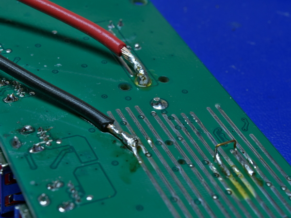
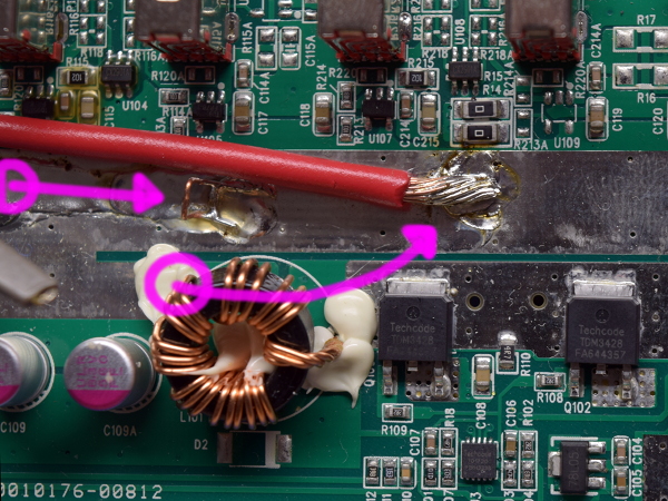
Since connecting my load to USB ports and dealing with individual per-port protections wouldn’t be practical, I decided to bypass the protections altogether by tapping directly into the ground plane and output filter circuit. I also gave myself a ground point for my oscilloscope probes in the bottom-right corner.
Looking at this image, I realize that I may have made a small but possibly significant mistake. By soldering the load’s positive wire directly to the output inductor’s lead, I’m feeding raw output noise into my load, which would have been filtered by the polymer caps had I soldered my positive load wire just about anywhere else on the 5V bus.
Noise Shelter
To shelter my test equipment from raw switching noise, I relocated the 5V test point an inch to the right and moved my red wire to the middle of the 5V bus on the top side.
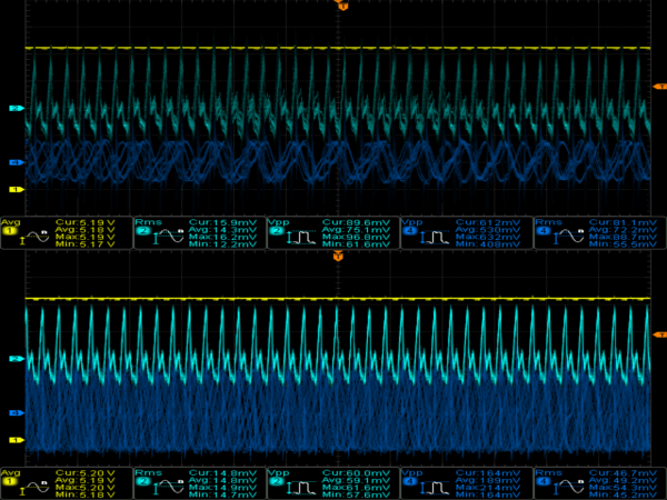
Did moving my positive wire to the top-side 5V pour, far behind the notch separating the inductor and polymer caps from the USB ports, make any difference? Let’s compare output noise under an 8A load and figure out whether I need to redo measurements over such a seemingly minor detail.
Subject To Change
What is the take-away from my before and after results? Between moving test points and fixing a sense amplifier stability issue in the DIY load, output RMS noise (cyan) remains unchanged at 14-15mV, while peak-to-peak noise drops from 90mV to 60mV mostly thanks to losing the highest-frequency transients. Noise on the DC-in side (blue) had a far more significant drop from 600mV to 200mV peak-to-peak and 72mV to 50mV RMS, which may have been mainly from my load’s hiccups. Also of note is that the AC adapter’s switching no longer appears correlated to the DC-DC converter’s.
There are too many significant changes, and spot-checking shows similar differences at other load levels too. It's time to throw out my old results and generate fresh ones.
-
andrewpong Could you look at anker 5 port chargers, especially those with PowerIQ and QuickCharge features?Reply -
Daniel Sauvageau Reply
As far as I know at the moment, Power IQ appears to be Anker's trademark for using device identification chips, quite possibly the same CX1901/2901 and equivalents everyone else use.20905501 said:Could you look at anker 5 port chargers, especially those with PowerIQ and QuickCharge features?
As for QuickCharge, PassMark sent me one of its USB-PD testers and I was told they MIGHT implement QuickCharge support in the future. Right now, I'm waiting to hear more about how likely that is to happen while I decide how I am going to use the tester in the future, which currently means pestering PassMark with bug reports and feature requests to enhance its versatility.
I did receive three adapters with QC 3.0 support and a plain 5-ports adapter, two from Aukey, two from Anker courtesy from Roger. I could do tear-downs and test them as regular 5V adapters for now, then revisit them once I have something to emulate the protocol with. I could certainly start that batch from the 5-ports non-QC one and pit it against SilverStone's UC01.
At the moment, I have two more cube-style generic adapters in the publication pipeline and I'm partly done putting together a third one about a house-brand unit. (Spoiler: that third one is disappointing for unusual reasons. Though the 'unusual' could simply be because I am breaking into a new form-factor category - at least for me - on that one.) -
andrewmtl This is awesome for the party, if you host a party that is around 10 ppl, then you will love this little device, by the way, I believe that also had 2-3 faster charging port!Reply -
Daniel Sauvageau Reply
As I pointed out in the tear-down, two ports have dedicated 2.4A (2.6-2.65A measured) output each and a second pair is sharing a single 2.4A e-fuse, each pair using a CH2311 charger ID chip. The rest all do 1.4A with various resistor ID schemes.20938782 said:This is awesome for the party, if you host a party that is around 10 ppl, then you will love this little device, by the way, I believe that also had 2-3 faster charging port!
For offices, parties and mobile devices/gadgetry hoarders where function and convenience far outweigh efficiency, this sort of device can become a necessity.
