DDR400 Kills Rambus: Shooting Star SiS 648 for P4
Features
By
Frank Völkel
published
Add us as a preferred source on Google
Get the Tom's Hardware Newsletter
Get Tom's Hardware's best news and in-depth reviews, straight to your inbox.
By submitting your information you agree to the Terms & Conditions and Privacy Policy and are aged 16 or over.
You are now subscribed
Your newsletter sign-up was successful
An account already exists for this email address, please log in.
Subscribe to our newsletter
Block Diagram Of The SiS 648
Below is a block diagram of the 648 chipset, which consists of a Northbridge (648) and and a Southbridge (963). Interestingly enough, SiS decided against single-chip technology, which it had implemented with its 735 chipset.
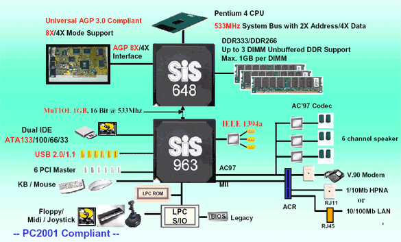
The block diagram shows the basic architecture of the SiS 648 chipset.
Northbridge of the SiS 648 chipset.
Southbridge SiS 963 of the 648 chipset.
Stay On the Cutting Edge: Get the Tom's Hardware Newsletter
Get Tom's Hardware's best news and in-depth reviews, straight to your inbox.
Current page: Block Diagram Of The SiS 648
Prev Page SiS 648: Alternative To Intel 845G Next Page Top-Notch Functions: DDR400, AGP 8x And USB 2.0
No comments yet
Comment from the forums
