3D DRAM Proposal Paves the Road for a Density Increase
Chip stacking for memory

Get Tom's Hardware's best news and in-depth reviews, straight to your inbox.
You are now subscribed
Your newsletter sign-up was successful
If there's one tech product where scaling doesn't work quite as well, it's DRAM. There are a number of reasons for this, the most important being the actual design of DRAM cells and how it relates to fabrication. But according to Lam Research, the end result of these scaling difficulties means that researchers in the DRAM field may be out of ways to increase DRAM's density scaling as early as five years from now.
It's in this context that Lam Research, a company specializing in semiconductor circuit design, has published a proposal for how future DRAM products may evolve. And that future may very well be 3D, so it seems that memory cubes aren't that far outside the realm of possibilities. According to the company, it'll take us around five to eight years to be able to design a manufacturable 3D DRAM device, leaving the world with a possible three-year gap between the moment 2D DRAM scaling ends and 3D DRAM scaling picks up.
Using their proprietary SEMulator3D software, Lam Research iterated on possible 3D DRAM designs. Their focus was on solving scaling and layer stacking challenges, capacitor and transistor shrinking, inter-cell connectivity, and via arrays (such as TSMC's TSV [Through Silicon Vias], which we've seen in other 3D semiconductor designs already). Finally, the company laid down the process requirements that enable fabrication of their proposed design.

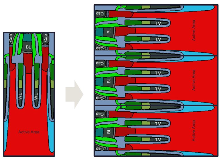
Due to the way DRAM cells are designed, it won't be possible to simply lay 2D DRAM components on their side in order to then stack them on top of each other. This happens because DRAM cells have a high aspect ratio (they're taller than they are thick). Laying them on their side would need lateral etching (and filling) capabilities that are beyond our current capacity.
But when you understand the architecture itself, you can change it and adapt it while attempting to flow around design constraints. This is easier said than done, however, and there's a reason we don't already have 3D DRAM.
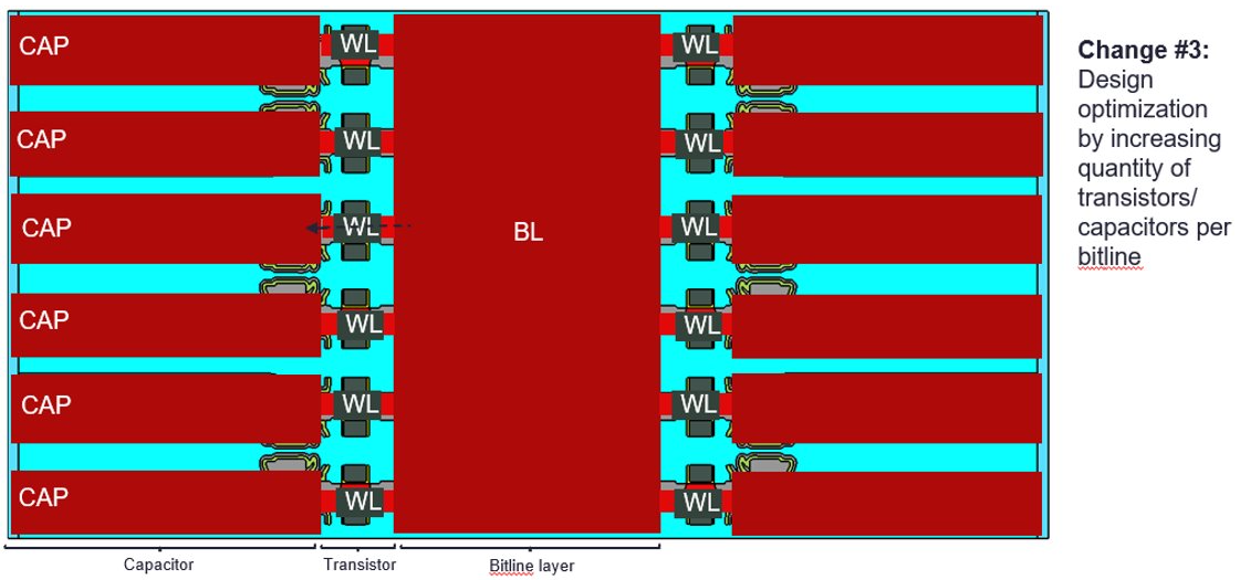
Current DRAM circuit designs need essentially three components: a bitline (a conductive structure that injects current); a transistor that receives the bitline's current output and serves as the gate controlling whether electrical current can flow into (and fill) the circuit; and a capacitor, where the current that flows through the bitline and transistor is ultimately stored in the form of a bit (0 or 1).
Lam Research used a few chip design "tricks" to reach a working architecture. For one, they moved the bitline over to the opposite side of the transistor; because the bitline is no longer surrounded by the capacitor, this means that more transistors can be connected to the bitline itself, improving chip density.

In order to maximize area density gains, Lam Research also applied a few state-of-the-art transistor manufacturing techniques. These include Gate-All-Around (GAA) forksheet designs, which Intel seems to be exploring for next-generation gating technologies. The redesigned DRAM architecture proposed by Lam research can then be stacked, with layers upon layers of the new DRAM cell design on top of one another in a process not unlike that of NAND.
But while NAND scaling is currently around the 232-layer mark, Lam Research estimates that the first generation of a 3D DRAM design such as its own would only leverage up to 28 stacked layers. With the architecture improvements and additional layering, Lam Research estimates that a two-node jump improvement in DRAM density can be achieved — with further improvements being possible through adding additional layers to the DRAM skyscraper. As we've seen in other fabrication technologies, the usage of a via array (the technology underpinning TSMC's TSV) is then used to interconnect individual layers.
There is however an immediate problem with the design proposed by Lam Research: There are no current manufacturing tools that can reliably fabricate the needed features. The company is quick to point out that DRAM design itself lives at the bleeding edge of today; improving and redesigning tools and processes is a common requirement. And as the company puts it, we still have time before we hit the DRAM scaling wall. Hopefully the required tools and expertise will arrive within that time-frame.
Get Tom's Hardware's best news and in-depth reviews, straight to your inbox.

Francisco Pires is a freelance news writer for Tom's Hardware with a soft side for quantum computing.
-
InvalidError DRAM is quite similar to NAND apart from the writing/erasing method and I have said several months ago that we'll eventually see multi-layered DRAM made in a similar manner.Reply
Not sure what the big deal is with "etching sideways" when conventional lithography lets you do fundamentally the same thing by adding layers of whatever material you need and then etching them to whatever shapes you need. -
Geef This isn't too much of a problem. PC memory hardly ever needs to be upgraded. For many years 8GB of memory was enough for everyone. Then it moved up to 16GB.Reply
For bigger needs like servers there are a ton of slots for memory so its not really an issue, if it is just change motherboards for more slots.
Maybe in 20+ years it might become an issue for servers but PCs will be just fine running at - double the memory every 10 years? - A 64 GB PC as a base model and gamers running 128GB. -
InvalidError Reply
The number of slots isn't the only problem. You also have the cost of platforms with more slots or slots that support higher density DIMMs. There are applications that can benefit from having more RAM but aren't necessarily worth having that much extra RAM at current prices. Then you have applications that already use all of the RAM that can be practically tossed at them and could use more if there was a cost-effective way of plugging it in. If you can cram 16X the amount of memory per chip, that opens up the possibility of stuffing all of the bandwidth mainstream CPUs and GPUs need in a single HBM-like chip stuffed directly on the CPU/GPU substrate or even 3D-stacked on a memory/cache/IO die/tile.Geef said:For bigger needs like servers there are a ton of slots for memory so its not really an issue, if it is just change motherboards for more slots.
And besides all of the above reasons and any others I may have missed, nobody is going to protest being able to buy 2-4X as much RAM for a given amount of money either. -
Diogene7 I would much, much prefer that they allocate ressources to develop manufacturing tools to scale up the manufacturing of Non-Volatile Memory (NVM) such as VCMA MRAM, or VG-SOT-MRAM (as per concept from European research center IMEC) to replace volatile DRAM as Non-Volatile Memory is a needed disruptive technology to enable so many improvements like « Normally-off Computing » : this is soooo much needed !!!Reply -
InvalidError Reply
DRAM in self-refresh mode is only 20-30mW per chip, a negligible part of system power next to the 10-70W it takes just to display a static screen between key presses depending on how large and how bright the screen is. Most modern motherboards waste more power on on-board RGB than necessary for DRAM self-refresh.Diogene7 said:I would much, much prefer that they allocate ressources to develop manufacturing tools to scale up the manufacturing of Non-Volatile Memory (NVM) such as VCMA MRAM, or VG-SOT-MRAM (as per concept from European research center IMEC) to replace volatile DRAM as Non-Volatile Memory is a needed disruptive technology to enable so many improvements like « Normally-off Computing » : this is soooo much needed !!!
If you want to reduce idle/standby power consumption, a better thing to focus on is reducing the number of background processes that needlessly wake up the CPU and its peripherals. -
hotaru251 Reply
for most ppl? sure.Geef said:PC memory hardly ever needs to be upgraded. For many years 8GB of memory was enough for everyone. Then it moved up to 16GB.
However the more we get to "ai" type stuff more ram will be needed. (again this is for niche use cases but they will exist)
has limitations as your memory traces get longer & your speed/latency suffer as result.Geef said:if it is just change motherboards for more slots. -
usertests Controversial opinion: I would like higher memory capacity for less money. Let's see $0.10/GB memory.Reply
Consumer memory requirements have mostly plateaued, suspiciously around the same time frame that cost per bit stopped reliably declining and memory prices zigzagged every few years.Geef said:This isn't too much of a problem. PC memory hardly ever needs to be upgraded. For many years 8GB of memory was enough for everyone. Then it moved up to 16GB.
For bigger needs like servers there are a ton of slots for memory so its not really an issue, if it is just change motherboards for more slots.
Maybe in 20+ years it might become an issue for servers but PCs will be just fine running at - double the memory every 10 years? - A 64 GB PC as a base model and gamers running 128GB.
https://jcmit.net/mem2015.htm
If everybody's memory suddenly quadrupled, we would have a good time. We still have 4 GB being sold in low-end laptops and tablets. Games could probably be made to use 64 GB soon, not necessarily as a requirement, but to brute force around slower storage. Stack a large amount of DRAM on a mega APU and that could be used for gaming or machine learning.
In servers/enterprise, many users could use more, and would also appreciate the cost per bit plummeting again.
If 3D DRAM octuples capacity/density at 8x the price, it doesn't matter that much. If it octuples at 0.5-2x the price, then things get interesting. -
Diogene7 ReplyInvalidError said:DRAM in self-refresh mode is only 20-30mW per chip, a negligible part of system power next to the 10-70W it takes just to display a static screen between key presses depending on how large and how bright the screen is. Most modern motherboards waste more power on on-board RGB than necessary for DRAM self-refresh.
If you want to reduce idle/standby power consumption, a better thing to focus on is reducing the number of background processes that needlessly wake up the CPU and its peripherals.
The « Normally-Off Computing » concept apply to the whole spectrum of computing devices and the benefits are not limited solely to lower power consumption, even though it is one of the important benefit, especially for battery operated devices (ex: IoT devices)
Yes one of the goal is to achieve overall lower system power consumption (through spintronics related technologies), but there is also the great advantage of much, much lower latency as you may not need (or at least less) need to load (shuffle) software/data from a slow non volatile storage device (HDD, SSD,…) to a fast volatile working memory (DRAM) : your Non-Volatile working Memory (NVM) (like MRAM) could be both used at the same time as fast, NVM DRAM and storage.
Your system only consume energy when it is doing a task, not when it is in idle, nor shut down, and is always immediately ready as soon as you turn on power (no boot time (or at least much less)) : I think that people don’t really realize how groundbreaking it would be because, as of 2023, such system doesn’t yet exist m, and therefore they never yet have the opportunity to experience the benefits of such a system (as Steve Jobs famoulsly said « A lot of times, people don't know what they want until you show it to them. »)
You could design an energy harvesting « bi-stable » systems (especially IoT devices, mobile devices,…) with gigabytes bi-stable, Non Volatile working memory/storage (VCMA MRAM, or VG-SOT-MRAM) and bi-stable color E-Ink display, with an embedded Artificial Neural Networks (ANN), for which the weights are stored in Non-Volatile SRAM/cache (VG-SOT-MRAM) : In Idle, your system wouldn’t consume any power, but as soon as a sensor is triggered, then your system wakes up, data go through the Non-Volatile ANN to decide what to do (compute), execute, and then go back to sleep.
For many infrequently triggered, battery operated IoT sensors it would be game changing : if the IoT device can harvest energy from the environment (small solar panel, vibration,…), and store it in a small battery, then it may provide enough energy to never have to manually recharge or change a non rechargeable coin cell battery in your devices. -
InvalidError Reply
Standby mode has existed for over 20 years and gives you the benefit of a computer that wakes up faster than the monitor can sync up with the video signal. Having a computer that is "instant on" is nothing new to people who can be bothered to use it.Diogene7 said:Your system only consume energy when it is doing a task, not when it is in idle, nor shut down, and is always immediately ready as soon as you turn on power (no boot time (or at least much less)) : I think that people don’t really realize how groundbreaking it would be because, as of 2023, such system doesn’t yet exist
What sort of energy-harvesting IoT device does sufficiently complex tasks that it needs so much RAM that self-refreshing RAM becomes a meaningful concern? Typical sensors don't really do much besides measure, transmit measurement, go back to sleep. You can do that sort of stuff in less than 1KB of (S)RAM... unless you are running a few million lines of bloat in the form of an OS when all you really need from it is a barebones network stack.Diogene7 said:For many infrequently triggered, battery operated IoT sensors it would be game changing : if the IoT device can harvest energy from the environment (small solar panel, vibration,…), and store it in a small battery, then it may provide enough energy to never have to manually recharge or change a non rechargeable coin cell battery in your devices.
The most popular IoT devices are things like voice assistants, smart plugs, doorbells, surveillance cameras, thermostats, etc., all of which wired/plugged-in, most of which always-on, continuously recording to catch trigger words or motion. Not much point in worrying about 30mW of self-refresh when the bus IO is drawing 300+mW. -
The Historical Fidelity Reply
Intel from 2016 is calling and asking where you were when they were losing money left and right producing non-volatile Optane memory.Diogene7 said:I would much, much prefer that they allocate ressources to develop manufacturing tools to scale up the manufacturing of Non-Volatile Memory (NVM) such as VCMA MRAM, or VG-SOT-MRAM (as per concept from European research center IMEC) to replace volatile DRAM as Non-Volatile Memory is a needed disruptive technology to enable so many improvements like « Normally-off Computing » : this is soooo much needed !!!