Adata Overclocks Its DDR5 Module to 8118 MT/s
Let the DDR5 overclocking contest begin.

DDR5 memory modules and supporting platforms are yet to hit the market, but DRAM houses have already started an informal DDR5 overclocking contest. Recently, Adata's XPG Overclocking Lab (XOCL) announced that it had managed to overclock the company's DDR5 memory module to 8,118 MT/s. This is the first time that a memory module house demonstrates overclocked DDR5 SDRAM sticks.
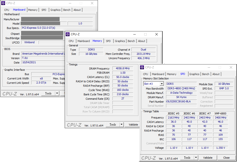
To hit a rather record data transfer rate, Adata's XPG Overclocking Lab (XOCL) took a pre-production 16GB DDR5 memory module based on ICs from SK Hynix with a stock data transfer rate of 4,800 MT/s and an unknown Intel Z690-based motherboard equipped with an undisclosed Intel's 12th Generation Core 'Alder Lake' processor. The module could hit 8104 MT/s and 8188 MT/s in single-channel mode and the system remained stable enough to load Windows and CPU-Z software.
Adata does not disclose what kind of cooling it used for the CPU and what voltage it set for the DDR5 module to get to 8188 MT/s. All the company demonstrated were CPU-Z screenshots.

Speaking of the module, it is necessary to note that we are indeed dealing with a pre-production unbuffered DIMM marked as AX5U5200C38 16G-BLA, so as the name suggests, the module was supposed to run at DDR5-5200 with CL38 CAS latency. Meanwhile, its SPD has an XMP-6800 CL46 entry at 1.35V, which is perhaps what Adata is preparing to launch in the foreseeable future. In any case, the default data rate featured by most DDR5 modules set to be released this year will be JEDEC standard 4800 MT/s.
So far, leading makers of memory chips like Micron, Samsung, and SK Hynix have demonstrated that their DDR5 memory chips could work at 7200 MT/s or even 8400 MT/s. Those experiments were conducted using equipment test equipment for DRAM chips or standalone DDR5 DRAM controllers and while such experiments reveal the potential of DRAM, they do not test memory ICs in real-world conditions using real-world workloads. Memory module houses followed the suite: Netac said it was developing DDR5-10000 modules back in April, whereas Adata said that it had managed to run DDR5 at 12600 MT/s in the lab back in August.
This time around Adata uses real (albeit pre-production) hardware to achieve a very high data rate and even launch Windows along with CPU-Z software. It will of course take some time before the company and its peers release actual DDR5-8200 memory modules, but at least we do know that even current-generation modules can work at extreme speeds.
Get Tom's Hardware's best news and in-depth reviews, straight to your inbox.

Anton Shilov is a contributing writer at Tom’s Hardware. Over the past couple of decades, he has covered everything from CPUs and GPUs to supercomputers and from modern process technologies and latest fab tools to high-tech industry trends.
-
wifiburger lol....Reply
that 8118MT/s might as well be DDR4 4000 or lower
50tcl cycles + 50trcd cycles, 100 cycles to get in/out data + Gear4 for the addressing
let's compare to bdie 4000 , 16tcl + 16trcd to get in/out data, yeah 32cycles at 4000MT/s
see the problem here ? 3x the latency -
TJ Hooker Reply
RAM timings are specified in clock cycles. A clock cycle at 8118 MT/s takes ~half as long as one at 4000 MT/s. So as CL of 50 at 8000 MT/s is equivalent to a CL of 25 at 4000 MT/s in real latency (12.5 ns). So first word latency is ~1.5x, not 3x. With an 8n prefetch, it takes 54 cycles to complete a single data burst (13.5 ns at 8000 MT/s), assuming the row was already open. The DDR4 would take 20 cycles, which would be 10ns at 4000 MT/s. So looking at it that way, the latency is now only 35% higher.wifiburger said:lol....
that 8118MT/s might as well be DDR4 4000 or lower
50tcl cycles + 50trcd cycles, 100 cycles to get in/out data + Gear4 for the addressing
let's compare to bdie 4000 , 16tcl + 16trcd to get in/out data, yeah 32cycles at 4000MT/s
see the problem here ? 3x the latency -
wifiburger Reply
you're calculation kinda make sense, but DDR5 is forced into Gear4 for addressing & commandsTJ Hooker said:RAM timings are specified in clock cycles. A clock cycle at 8118 MT/s takes ~half as long as one at 4000 MT/s. So as CL of 50 at 8000 MT/s is equivalent to a CL of 25 at 4000 MT/s in real latency (12.5 ns). So first bit latency is ~1.5x, not 3x. With an 8n prefetch, it takes 54 cycles to complete a single data burst (13.5 ns at 8000 MT/s), assuming the row was already open. The DDR4 would take 20 cycles, which would be 10ns at 4000 MT/s. So looking at it that way, the latency is now only 35% higher.
if it was only 35% higher, we would of not got these early leaks on DDR5 showing 140ns for latency vs 40ns, 70ns DDR4 numbers. -
TJ Hooker Reply
I'm not sure which leaks you are referring to, but in general if the leaks are using DDR5 running at JEDEC spec then their timings are going to be pretty loose (as seems to always be the case with JEDEC timings). E.g. for DDR4 4800 the CL would be 40. Unless they're comparing it to DDR4 that's also running at JEDEC spec, it's not really a fair comparison. The max JEDEC speed for DDR4 is 3200 MHz as far as I know, with a CL of 20. Comparing those two, the difference in real CL should be 33%, at least on paper.wifiburger said:if it was only 35% higher, we would of not got these early leaks on DDR5 showing 140ns for latency vs 40ns, 70ns DDR4 numbers.