AMD and Nvidia GPUs Consume Lion's Share of TSMC's CoWoS Capacity

MI250X
(Image credit: AMD)

TSMC is on track to expand its chip on wafer on substrate (CoWoS) advanced packaging capacity by almost two times by the end of 2024, but even then Nvidia will consume half of capacity that the foundry is expected to have then, according to DigiTimes.

TSMC reportedly intends to expand its CoWoS capacity from 8,000 wafers per month today to 11,000 wafers per month by the end of the year, and then to around 20,000 by the end of 2024. But it looks like even then Nvidia will use around half of the capacity that TSMC will have, DigiTimes claims, citing sources familiar with the matter. Meanwhile, AMD is also trying to book additional CoWoS capacity for next year.

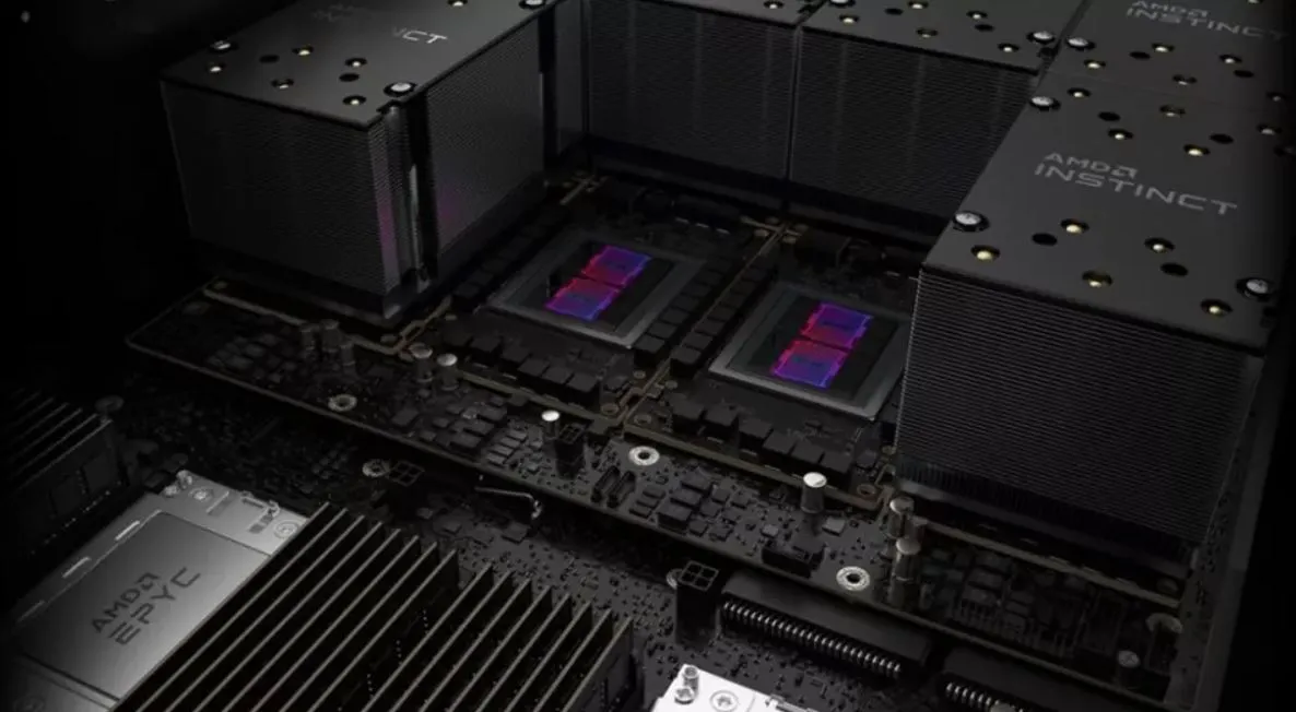
Megatrends like 5G, artificial intelligence (AI), and high-performance computing (HPC) are driving adoption of highly complex multi-chiplet designs like AMD's Instinct MI300 or Nvidia's H100. It is widely considered that Nvidia is the main beneficiary of the thriving demand for AI-bound compute GPUs, and that it controls over 90% of compute GPU shipments for new deployments. As a result, TSMC is struggling to meet demand for its CoWoS advanced packaging solutions.

TSMC currently has the capacity to process roughly 8,000 CoWoS wafers every month. Between them, Nvidia and AMD utilize about 70% to 80% of this capacity, making them the dominant users of this technology. Following them, Broadcom emerges as the third largest user, accounting for about 10% of the available CoWoS wafer processing capacity. The remaining capacity is distributed between 20 other fabless chip designers.

Packaging equipment for CoWoS and other advanced packaging technologies require specialized production tools, and they have lead times between three and six months. That means TSMC's ability to rapidly expand its CoWoS capacity is limited.

(Image credit: TSMC)

Last week TSMC opened its Advanced Backend Fab 6 facility, which is set to expand its advanced packaging capacity both for its frontend 3D stacking SoIC (CoW, WoW) technologies as well as backend 3D packaging methods (InFO, CoWoS), but for now the fab is ready for SoIC. The Advanced Backend Fab 6 has the ability to process around one million 300-mm wafers per year and carry out over 10 million hours of testing annually, with cleanroom space that is larger than the combined cleanroom spaces of all other TSMC advanced packaging facilities.

Among the most impressive features of the Advanced Backend Fab 6 is the extensive five-in-one intelligent automated material handling system. The system controls the production flow and detects defects instantly, increasing yield. This is crucial for complex multi-chiplet assemblies like the AMD's MI300, as packaging defects immediately render all chiplets unusable, leading to significant losses. With data processing capabilities 500 times faster than average, the facility can maintain comprehensive production records and track every die it processes.

Nvidia uses CoWoS for its highly successful A100, A30, A800, H100, and H800 compute GPUs. AMD's Instinct MI100, Instinct MI200/MI200/MI250X, and the upcoming Instinct MI300 also use CoWoS.

TSMC

(Image credit: TSMC)
Anton Shilov
Freelance News Writer

Anton Shilov is a Freelance News Writer at Tom’s Hardware US. Over the past couple of decades, he has covered everything from CPUs and GPUs to supercomputers and from modern process technologies and latest fab tools to high-tech industry trends.

  • Kamen Rider Blade
    Not surprised, they honestly need to triple their CoWoS packaging capacity given the ever increasing popularity of the design benefits of chip stacking.
    Reply