Ericsson processors built on 'Intel 4' process node beat Meteor Lake to deployment
IDM 2.0 is finally getting somewhere.

Get Tom's Hardware's best news and in-depth reviews, straight to your inbox.
You are now subscribed
Your newsletter sign-up was successful
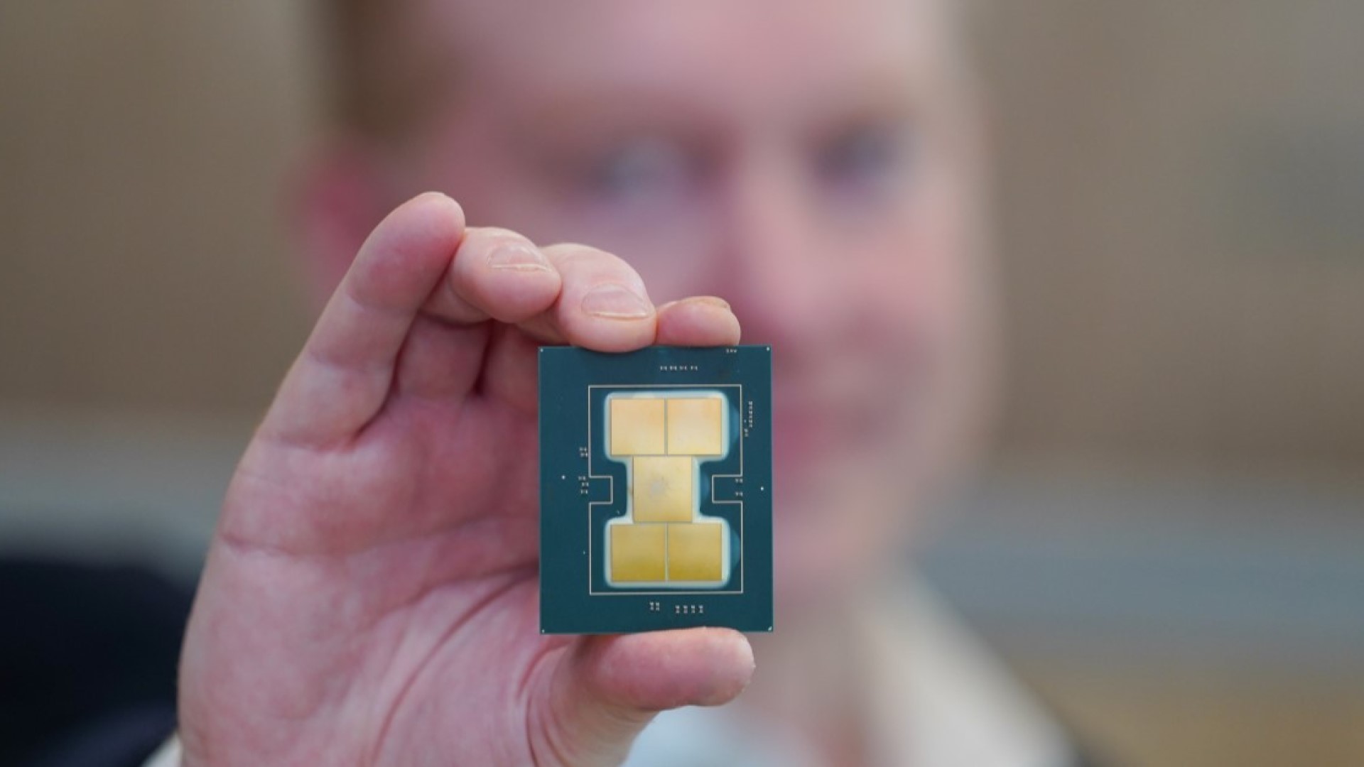
Intel's biggest foundry customer right now is arguably Ericsson, a company that deals in networking and 5G chips. Ericsson's latest RAN Compute processors are utilizing the Intel 4 process node, the same node that's used for Intel's upcoming Meteor Lake CPU tile, and Ericsson apparently beat Intel to market. This new partnership is the latest bit of good news for Intel's IDM 2.0 strategy, which aims to make Intel the second-best foundry in the world by 2030 — TSMC being first.
That Ericsson was teaming up with Intel to fab processors isn't anything new, as the company announced in July that a future generation of 5G chips would be fabbed on 18A, which is due in 2025. This Intel 4-fabbed processor was actually hinted at all the way back in February 2022 on a roadmap, but we didn't know it was being made on Intel 4 at the time. Now it's official.
According to Ericsson's internal testing, its RAN Compute chips made on Intel 4 use "30 to 60 percent less power compared to industry benchmarks." That info isn't as useful as a chip-to-chip comparison would be, but Ericsson's message is clear enough: Its new processors are very efficient. It's implied that Intel 4 is a key reason why these chips are so efficient, but Ericsson's press release doesn't come out and say it explicitly.
The new chips also have much improved performance, with the high-capacity 6672 and 6372 processors having four times the capacity of their predecessors. The efficiency-focused 6678 and 6671 routers also add AI technology into the mix, which has been 2023's top tech buzzword. Ericsson also boasts about its Open RAN architecture, which seeks to make networking less proprietary, more open, and able to work with a variety of server chips, whether they're running x86 or ARM or something else.
Although AMD is pretty skeptical of Intel's IFS business and its ability to succeed, this Ericsson-Intel partnership is a clear win for Intel. It also won a defense company contract for 18A chips back in 2021, an order from a big datacenter client to make processors on the Intel 3 node in January of this year, and last April even scored a deal with Arm to fab smartphone chips on 18A. If IFS continues to bear fruit, Intel could be in great shape over the coming years.
Get Tom's Hardware's best news and in-depth reviews, straight to your inbox.

Matthew Connatser is a freelancing writer for Tom's Hardware US. He writes articles about CPUs, GPUs, SSDs, and computers in general.
-
Order 66 what a surprise, a company beat intel to market. at least the current 10nm+++ isn't as bad as the 14nm+ (I don't remember how many generations 14nm spanned) of yesteryear.Reply -
JTWrenn Beat to market? They are two totally different markets. This is like comparing the next gen wifi to next gen desktops. It doesn't make any sense.Reply
In short there was no race, and they are much less complicated chips so it makes sense. If anything Intel used Ericsson as a test bed to work out their Intel 4 node. -
Order 66 Reply
good point, I just thought it was funny that Meteor Lake has been known for what seems like forever and it has yet to launch. I also just thought that Intel would have been the first to launch anything using their technology.JTWrenn said:Beat to market? They are two totally different markets. This is like comparing the next gen wifi to next gen desktops. It doesn't make any sense.
In short there was no race, and they are much less complicated chips so it makes sense. If anything Intel used Ericsson as a test bed to work out their Intel 4 node. -
bit_user Reply
They don't need the same amount of production volume.Order 66 said:what a surprise, a company beat intel to market.
Also, when they say they have it "on the market", I'll bet it just means they're shipping it to their customers (i.e. makers of 5G routers & base stations). Intel has been shipping Meteor Lake to its customers (i.e. system-builders) for many months, already. On that basis, it's a flawed comparison.
Intel 4 is what they used to call 7 nm. I think it's a EUV node, whereas Intel 7 (formerly 10 nm) is DUV.Order 66 said:at least the current 10nm+++ -
Order 66 Reply
This intel 4 and 7 is so confusing trying to figure out what the nanometer equivalent is.bit_user said:Intel 4 is what they used to call 7 nm. I think it's a EUV node, whereas Intel 7 (formerly 10 nm) is DUV. -
bit_user BTW, the first public Intel 4 chip was supposedly Horse Creek - a quad-core RISC-V SoC that was meant to ship on SiFive's HiFive Pro P550 dev boards:Reply
https://liliputing.com/sifive-hifive-pro-p550-dev-board-coming-this-summer-with-intel-horse-creek-risc-v-chip/
...still not shipping, though. What a disappointment. -
DavidC1 Reply
It don't matter. Samsung, TSMC doesn't use the nm naming scheme anyway. They deviated from the nm naming since "20nm".Order 66 said:This intel 4 and 7 is so confusing trying to figure out what the nanometer equivalent is.
That's why TSMC calls it N3 not 3nm, and Samsung uses whatever nonsense naming they use. -
kjfatl It reached the point that Intel was the only player using NM so they gave up and began using a numbering scheme similar to that used by TMSC and the other major players in the market.Reply
This is little different that Comcast advertising "This is the next generation 10G Network. Only from Xfinity" -
dimar I'd like someone to finally make power efficient 10GbE+ ethernet switches. (or at least 5GbE)Reply -
kjfatl You don't need them with Comcast. Their 10G network maxes out at about 1.2G.Reply
It's their 10th Generation of Cable modems, or something like that.
The intent from Comcast is to deceive the uninformed customer, just like TSMC's N3 moniker was to make you think they were using a 3nm process for their 7nm silicon.
