Intel Dishes on Alder Lake-S: First x86 Hybrid CPU for Desktops
The big.LITTLE CPU design comes to desktop PCs.
Among many other announcements (full breakdown here), Intel announced at its Architecture Day 2020 that the company would release its Alder Lake-S processors for the desktop PC in 2021. This marks the first time that Intel has brought its x86 hybrid architecture, which merges the use of both larger and smaller cores, to the mainstream desktop platform. Intel also unveiled the broad strokes of its Client 2.0 design initiative that will leverage more mix-and-match architectures in the future.
Intel's Alder Lake-S architecture features a design reminiscent of ARM's big.LITTLE (half-heartedly branded Big-BIGGER by Intel) with the larger cores used primarily for high-priority work, while the smaller cores execute less-intensive and background tasks and workloads. Intel didn't share many fine-grained details on the new chip, but did say Alder Lake-S will feature a combination of Golden Cove cores and Atom Gracemont cores. Given our current knowledge of Intel's roadmaps, we feel confident that these chips will come after the Rocket Lake chips that are next in line for the desktop PC.
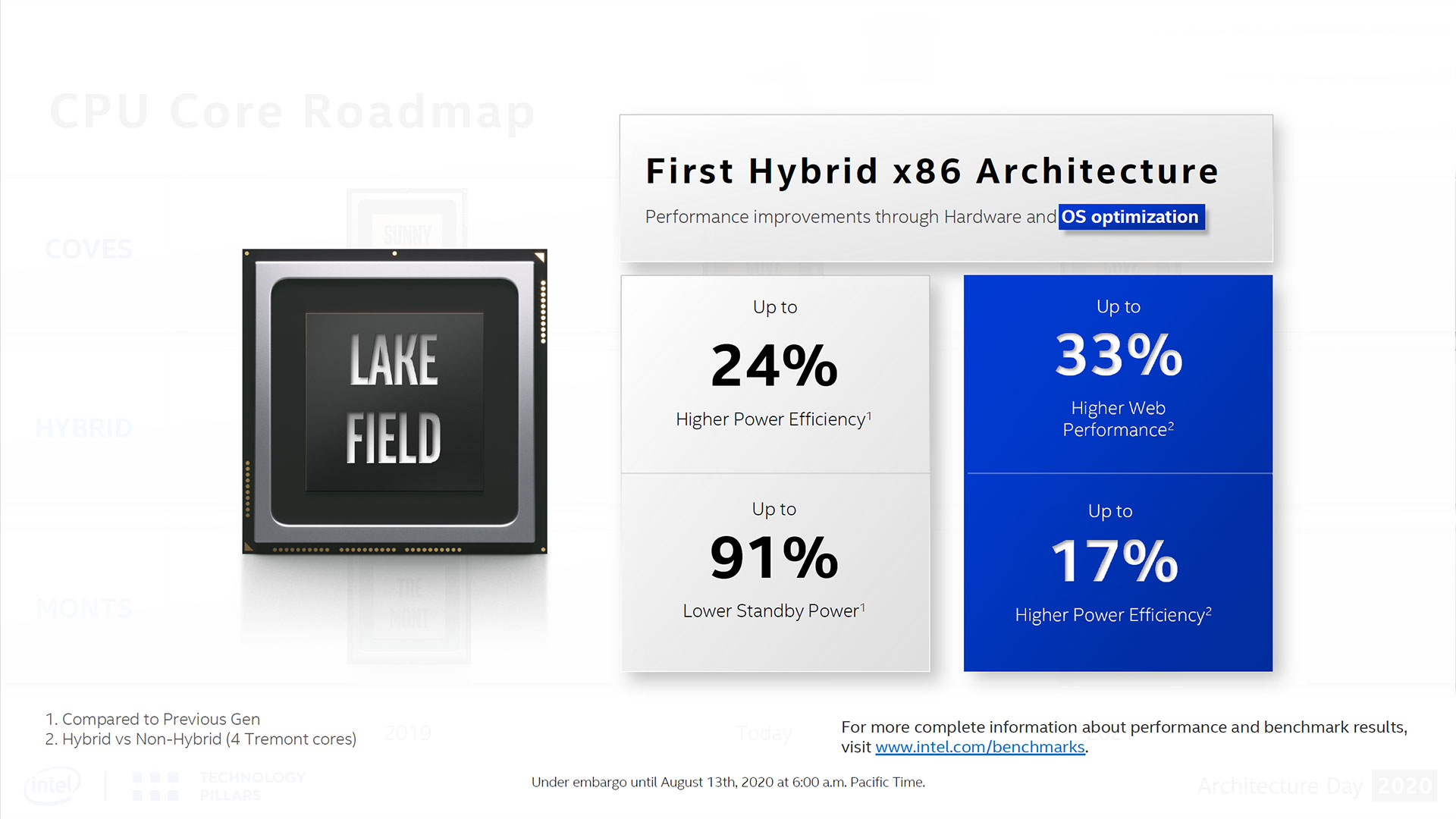
Intel pioneered the x86 hybrid architecture with its Lakefield chips, with those inaugural models coming with one Sunny Cove core paired with four Atom Tremont cores. Intel designed Lakefield for mobile devices, so retaining a snappy, responsive feel to the device was important, but power efficiency was also of the utmost performance to preserve battery life. Intel says it will discard that efficiency focus for its Alder Lake-S chips and tune for performance instead, which would certainly be an easier task due to the enhanced power budget and more robust thermal solutions available on the desktop.

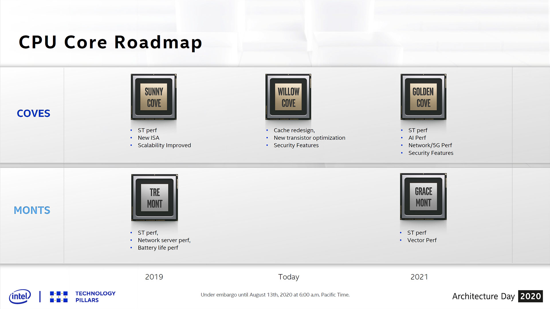
A pair of higher-performance cores is a good place to start, and, compared to Lakefield, both the high- and low-performance Alder Lake-S cores take a step forward to newer microarchitectures. Alder Lake-S actually jumps forward two 'Cove' generations compared to the 'big' Sunny Cove cores found in the shipping Lakefield chips. The big Golden Cove cores come with increased single-threaded performance, AI performance, Network and 5G performance, and improved security features compared to the Willow Cove cores that debut with the Tiger Lake processors later this year.
Meanwhile, Alder Lake's smaller Gracemont cores jump forward a single Atom generation and offer the benefit of being more power and area efficient (perf/mm^2) than the larger Golden Cove cores. Gracemont also comes with increased vector performance, a nod to an obvious addition of some level of AVX support (likely AVX2). Meanwhile, the larger Golden Cove cores should support AVX-512. That split instruction set support could portend optimizations to the hardware-aware scheduler in the operating system, which we'll cover shortly.
In its new roadmap, Intel also lists improved single-threaded performance for the Gracemont cores, but removed the “frequency” bullet point that was present when it unveiled the broad outlines of the Gracemont cores in 2018 at its previous Architecture Day.
Intel hasn't indicated which process node it will use for either of Alder Lake's cores, or if they will come in a 3D-stacked package like the Lakefield chips. Aside from improved battery life, one of Intel's primary mobile-centric design aspirations for Lakefield was to reduce the footprint of the chip package.
Get Tom's Hardware's best news and in-depth reviews, straight to your inbox.
The smaller footprint on Lakefield enabled smaller, thinner, and lighter mobile designs by shrinking the size of the chip package with 3D stacking, but Intel doesn't have the same footprint concerns on the desktop. As such, Intel wouldn't necessarily have to use the cost-increasing Foveros 3D packaging technique to bring the processors to market. Instead, the chipmaker could use a single monolithic die with two kinds of cores, a chiplet-based architecture composed of separate compute chiplets for each type of core, or stick with 3D Foveros packaging. Only time will tell.
| Processor | Big Cores | Small Cores | GPU Cores |
|---|---|---|---|
| Alder Lake-S | 8 | 8 | 1 |
| Alder Lake-S | 8 | 6 | 1 |
| Alder Lake-S | 8 | 4 | 1 |
| Alder Lake-S | 8 | 2 | 1 |
| Alder Lake-S | 8 | 0 | 1 |
| Alder Lake-S | 6 | 8 | 1 |
| Alder Lake-S | 6 | 6 | 1 |
| Alder Lake-S | 6 | 4 | 1 |
| Alder Lake-S | 6 | 2 | 1 |
| Alder Lake-S | 6 | 0 | 1 |
| Alder Lake-S | 4 | 0 | 1 |
| Alder Lake-S | 2 | 0 | 1 |
*Specifications in the above table are not confirmed
The combination of the two types of cores gives Intel a dizzying number of possible configuration options. We do know that 12 possible Alder Lake-S configurations have been listed to a patch for the open-source Coreboot (a lightweight motherboard firmware option). This listing outlines various combinations of the big and little cores in different chip models, with some models even using only the larger cores (possibly for high-performance gaming models), but that doesn't guarantee that all (or any) of those potential configurations will come to market. However, given that Intel will likely deploy Alder Lake as a top-to-bottom solution for its mainstream desktop platform, we're sure there will be numerous options.
Lakefield served as a proving ground not only for Intel's 3D Foveros packaging tech but also as an enabler for the software and operating system ecosystem. At its Architecture Day, Intel outlined the performance gains above for the Lakefield chips to highlight the promise of hybrid design. Still, the results come with an important caveat: These types of performance improvements are only available through both hardware and operating system optimizations. That's because unlocking maximum efficiency requires the operating system and applications to be aware of the architecture so they can target threads to the correct cores.
Due to the use of both faster and slower cores that are both optimized for different voltage/frequency profiles, the operating system and applications have to have an awareness of the architecture to ensure they direct the workloads to the correct core. For instance, if a latency-sensitive workload like web browsing lands in a slower core, performance will suffer. Likewise, if a background task is scheduled into the fast core, some of the potential power efficiency gains are lost.
There's already plenty of work underway in both Windows and various applications to support that technique via a hardware-guided OS scheduler. Still, the current format for Intel's Lakefield relies upon both cores supporting the same instruction set. Intel Chief Architect Raja Koduri mentioned that a new "next-generation" hardware-guided OS scheduler that's optimized for performance would debut with Alder Lake, but didn't provide further details. This next-gen OS scheduler could add in support for targeting cores with specific instruction sets to support a split implementation, but that remains to be seen.
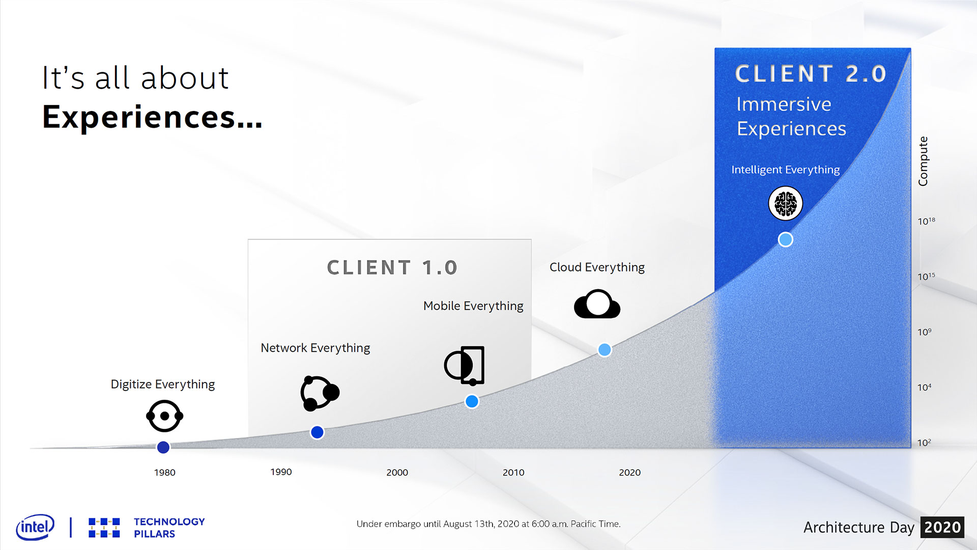
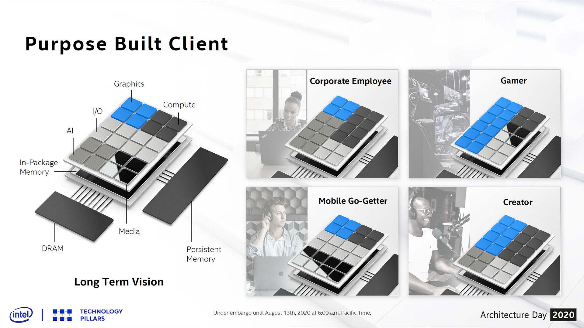
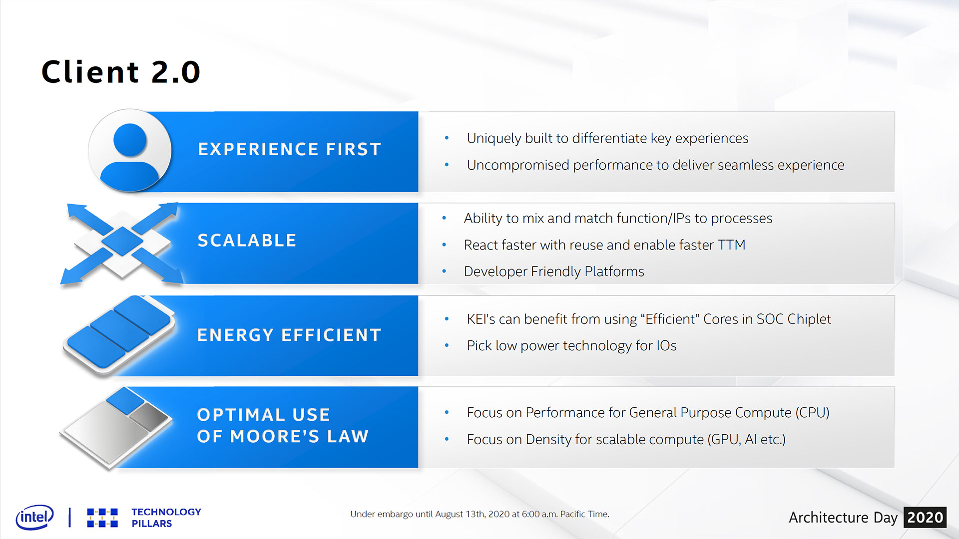
Intel's move to an x86 hybrid architecture could be seen as risky in the face of AMD's continuous onslaught of chiplet-based processors. Still, it appears Intel could remain committed to hybrid architectures in the future. As part of Architecture Day, the company had a short presentation outlining the broad strokes of its new Client 2.0 initiative. This initiative strives to tie several of Intel's newest technologies into a new design methodology for its processors, with the ultimate goal being a faster time to market for scalable, purpose-built devices.
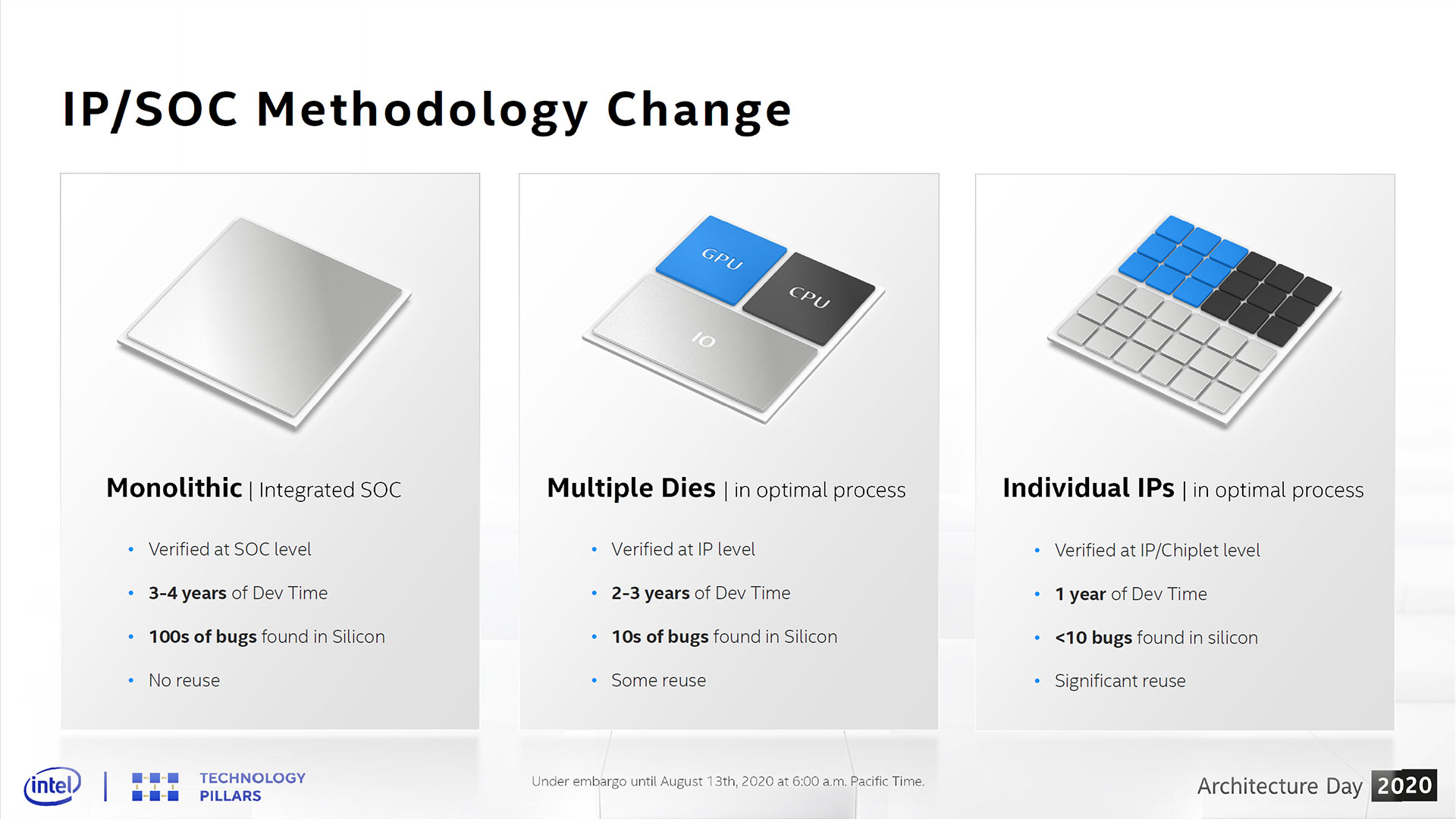
Intel's processors have historically relied upon monolithic single-die, general-purpose SoCs. In contrast, the Client 2.0 approach leverages many of the new technologies that Intel has developed, like advanced packaging, interconnects, and new memory technologies while layering in 'extreme innovation' in virtualization and advanced software APIs to enable its new focus on die disaggregation (the splitting of various functions and IP to differing process nodes).
The Client 2.0 design methodology aims to shrink the amount of time it takes to develop a product from the 3-4 years of the current design flow down to a single year, which improves flexibility and enables the company to rapidly shift products based on unforeseen circumstances – like delayed process nodes. The approach is also designed to reduce validation time, and we imagine it will also help to reduce cost.
Much of the benefit from the Client 2.0 approach comes from significant reuse of Intel's various IP technologies across the full breadth of its product stack, as opposed to customized implementations for each microarchitecture. As you can see in the album above, this method uses many of the same design tenets as the chiplet-based 'multiple-dies' approach that Intel is already moving to now, but with what appears to be a single-die approach tied to different tiers of external memory.
However, given that this is merely the first vague mention of the Client 2.0 initiative, Intel didn't provide further details. The company promises further details in the future. In either case, it's clear that Intel is firmly committed to mix-and-match designs that extend even beyond today's chiplet-based architectures, so it's safe to say that hybrid x86 architectures will become a mainstay in the company’s future product lines.

Paul Alcorn is the Editor-in-Chief for Tom's Hardware US. He also writes news and reviews on CPUs, storage, and enterprise hardware.
