Intel Unveils 10nm Atom Tremont Microarchitecture
Intel unveils its next-gen 10nm Atom microarchitecture
Intel pulled back the veil on its 10nm Tremont Atom architecture today at the Linley Fall Processor Conference. Intel's ULP (ultra-low power) architectures don't grab the flashbulbs like its venerable Core series of chips, but Atom processors power an untold number of low-power devices, like micro-servers, tablets, and Internet of Things (IoT) equipment. These segments still serve as a bastion for Intel, as AMD doesn't have competitive chips to tackle these areas.
Intel's move to the 10nm Atom Tremont architecture begins with a focus on single-threaded performance but also brings other big improvements to bear, like the addition of L3 cache, a first for Atom, new power management enhancements that complement improved performance-per-watt, bolstered security, and support for new instructions.
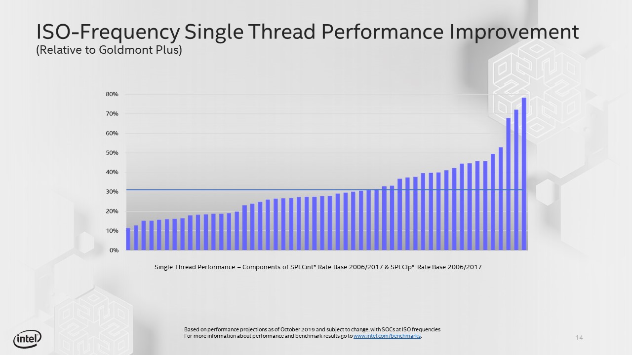
Intel claims the culmination of these efforts results in up to 30% more IPC (at ISO frequencies) for Tremont compared to the previous-gen Goldmont Plus architecture (SPEC). Unfortunately, Intel isn't revealing its clock speeds yet, so the increased IPC may give it room to accommodate lower frequencies that come as a byproduct of the new and yet-to-be-refined 10nm process, much like we see with Ice Lake processors.
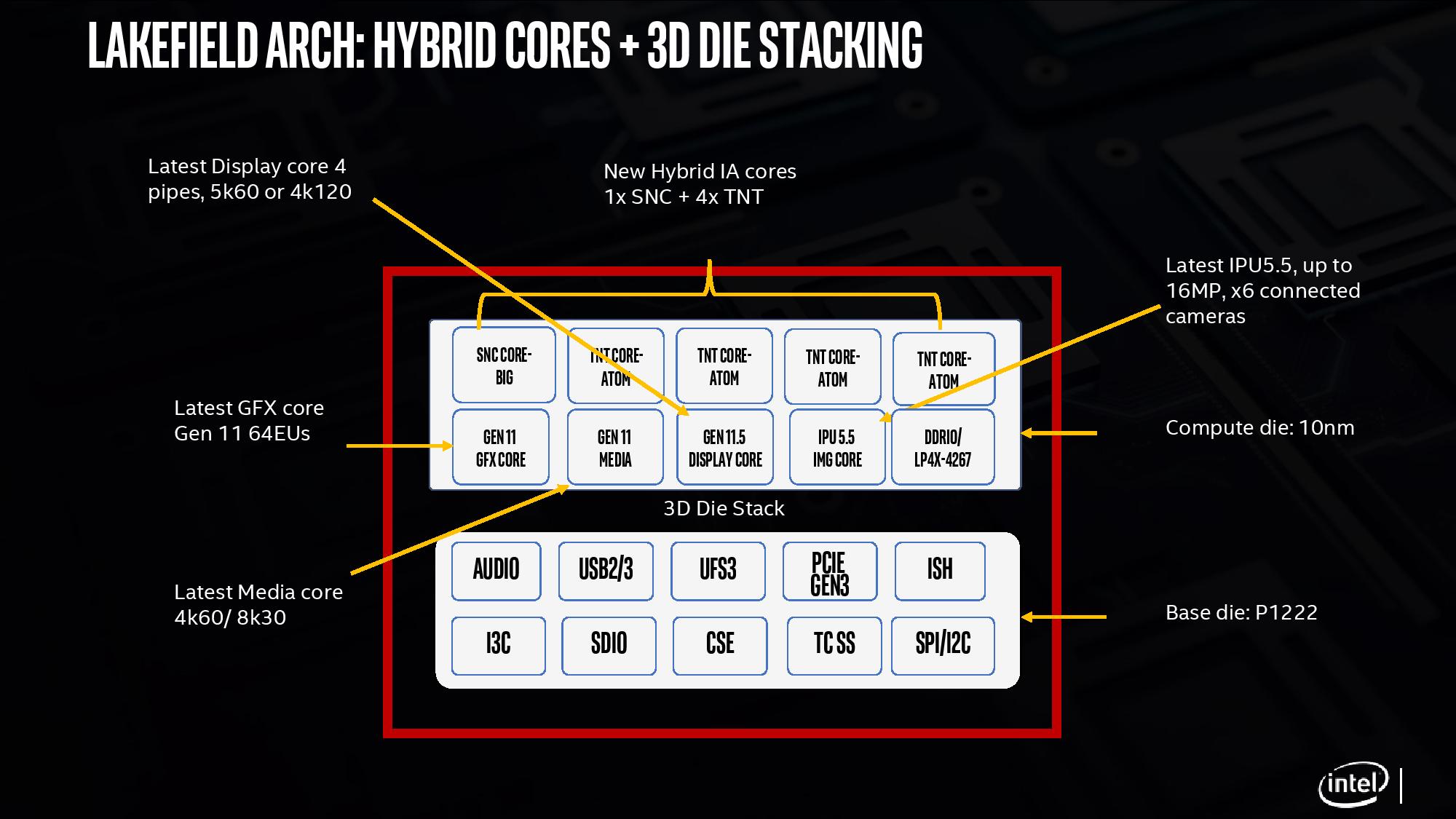
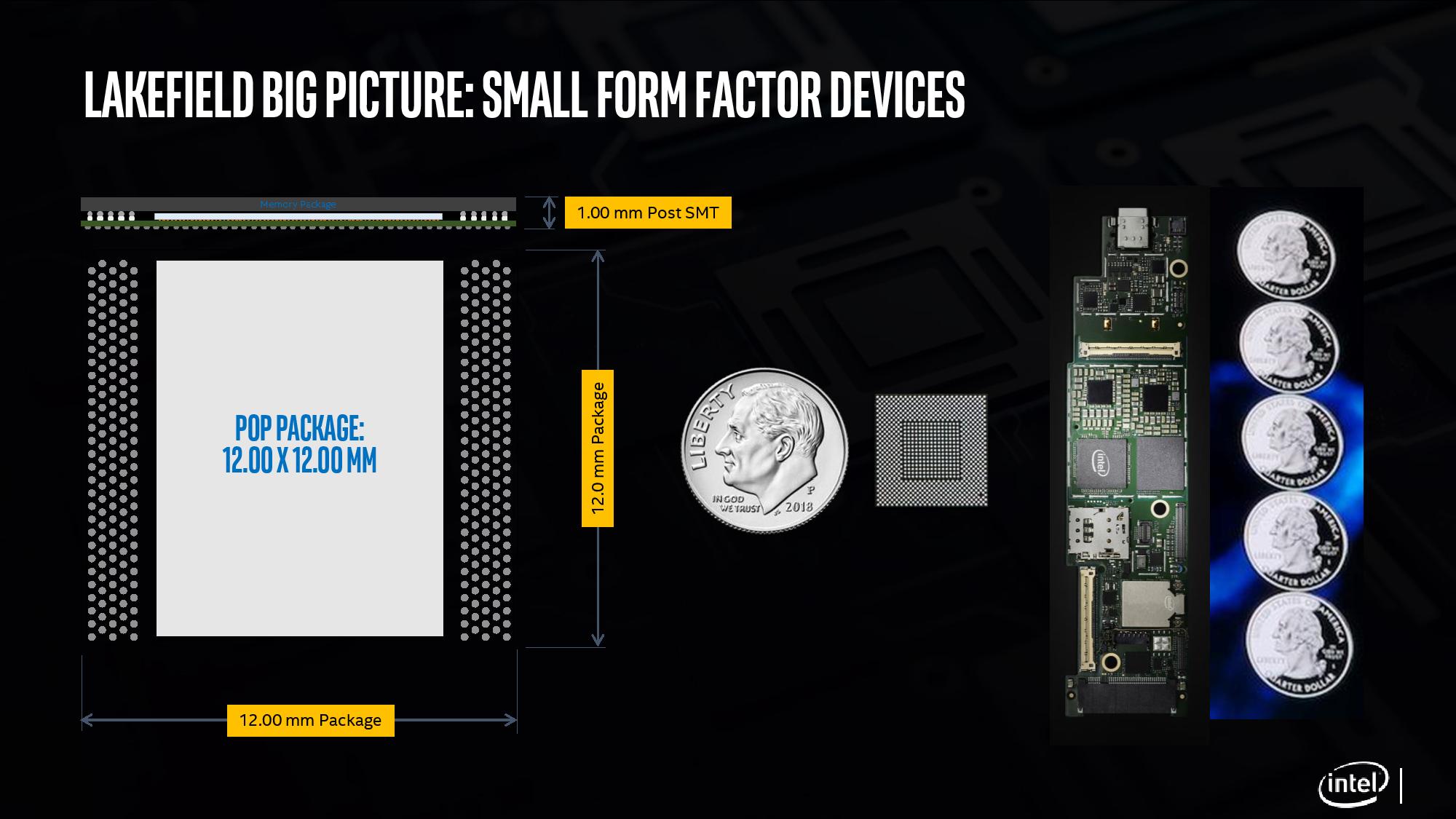
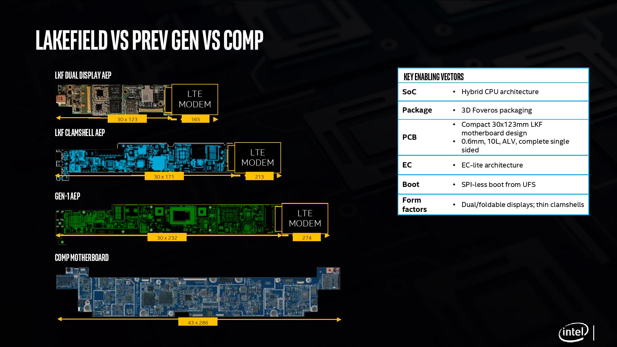
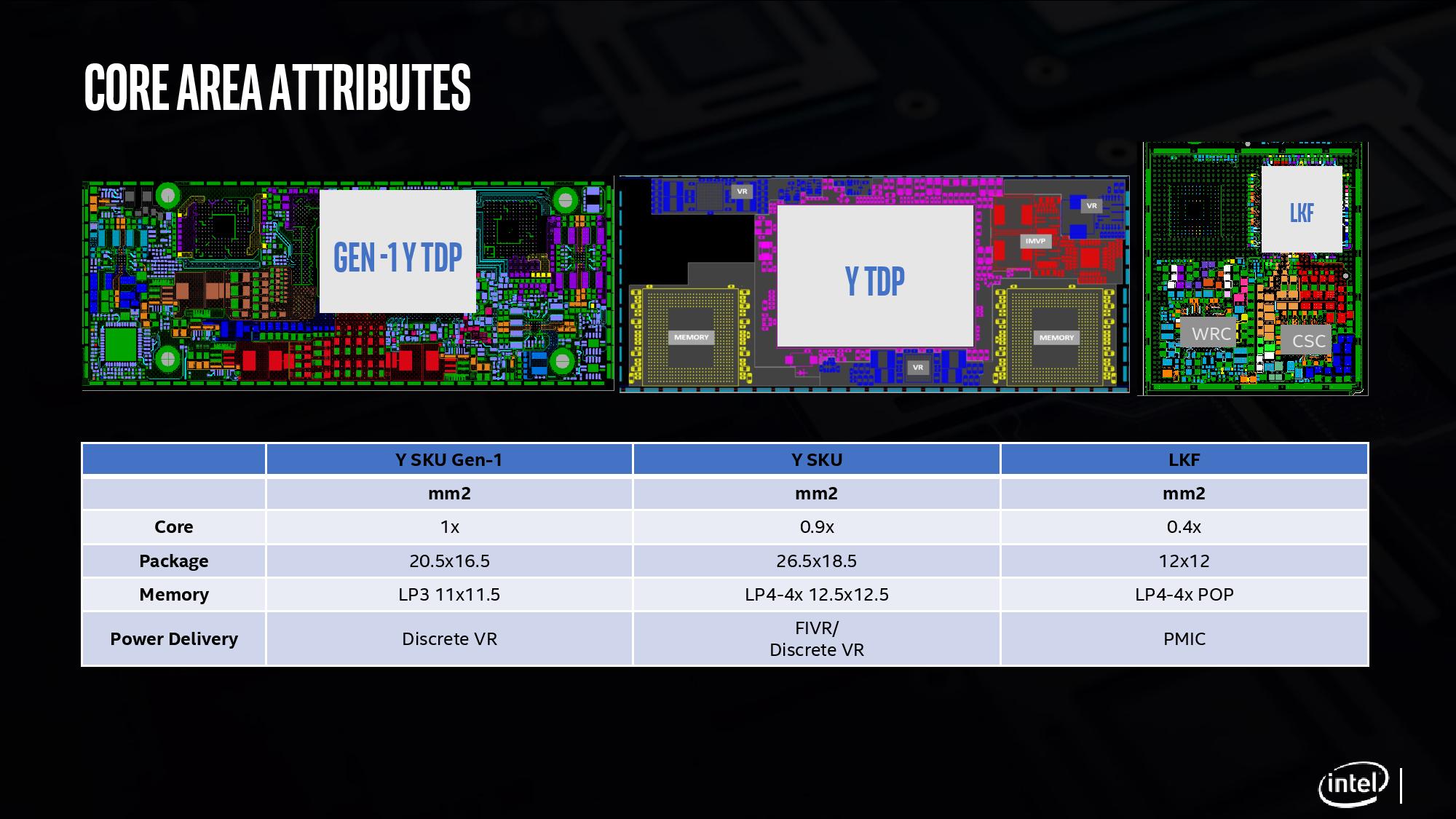
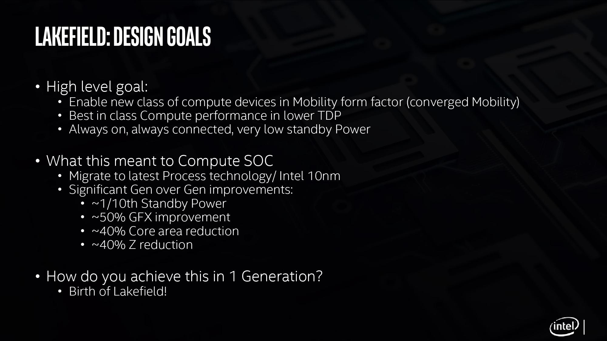
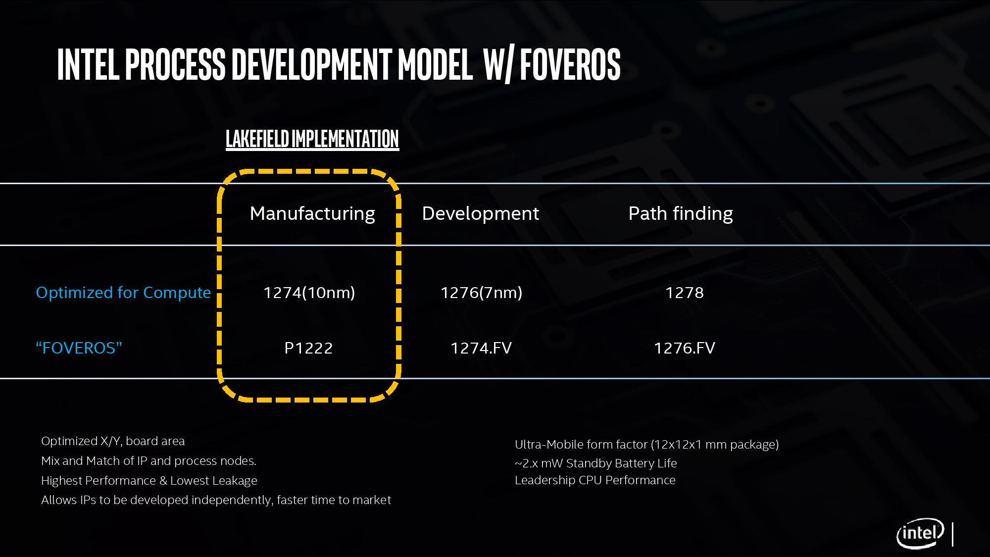
Intel's coming 3D-stacked Lakefield processors, like seen in Microsoft's Surface Neo devices, will feature four low-power Tremont cores paired with one high-performance Sunny Cove core in a hybrid approach glued together with Foveros technology. This approach allows Intel to offer an incredible amount of processing power at low power in ultra-dense designs.
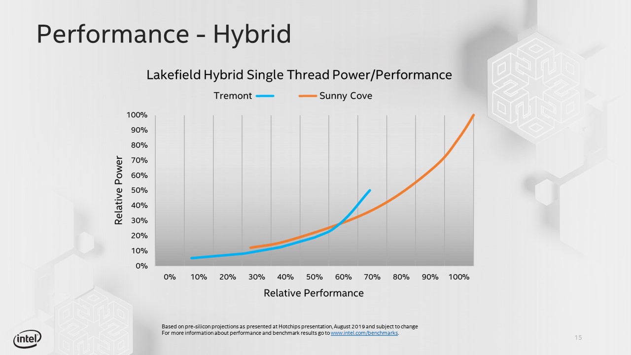
This approach allows Intel to meld together two different architectures to capitalize on the low-power and efficiency of the Tremont Atom cores and the high performance of the Sunny Cove core, thus creating a combination similar to an ARM big.LITTLE processor, which Intel calls a "hybrid x86 architecture."
But behind this blending of two distinct architectures to enable new levels of performance density and power efficiency lies the Tremont architecture, which will also find its way into numerous other processors in traditional form factors. Let's take a closer look at Intel's first 10nm low-power processing cores.
Intel Tremont Single-Threaded Performance
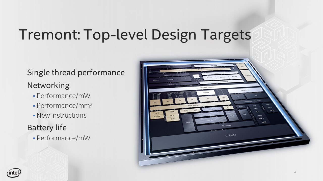
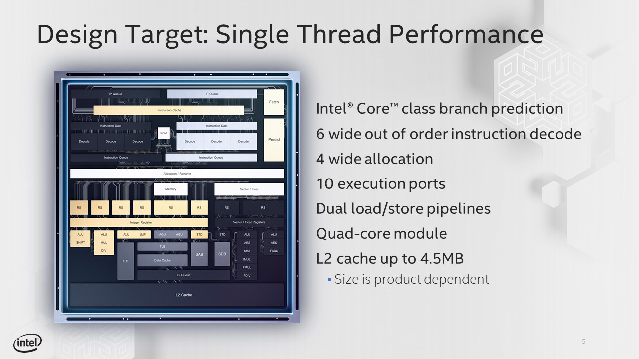
Intel's overarching design targets include a focus on single-threaded performance paired with improved power efficiency and performance density for the networking components that tie the various compute elements together.
Get Tom's Hardware's best news and in-depth reviews, straight to your inbox.
Intel beefed up Tremont's branch predictor to what it calls "Core-class" levels of performance, meaning the Atom cores will have nearly the same accuracy as their high-power Sunny Cove Core family counterparts. This is accomplished with a new dual-stage branch prediction implementation, though Intel isn't specifying which types of predictors it is using (TAGE is a likely suspect for the second stage).
The architecture can decode up to six out-of-order x86 instructions, and features four-wide allocation and retire, along with dual load/store pipelines.
The chips will come with four-core modules that share an L2 cache that can be up to 4.5MB, but will vary based on specific products.
Intel Tremont Front End (Fetch, Predict, Decode)
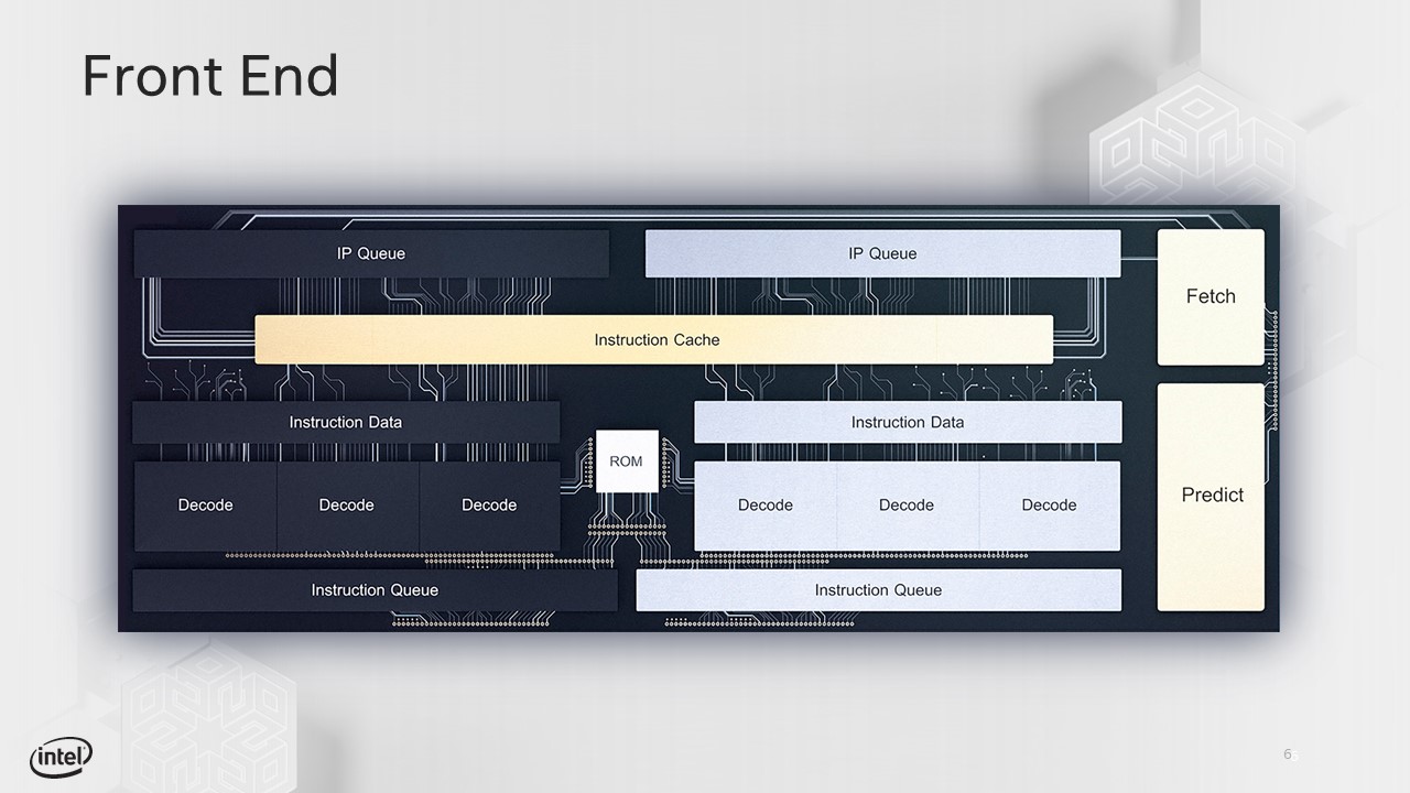

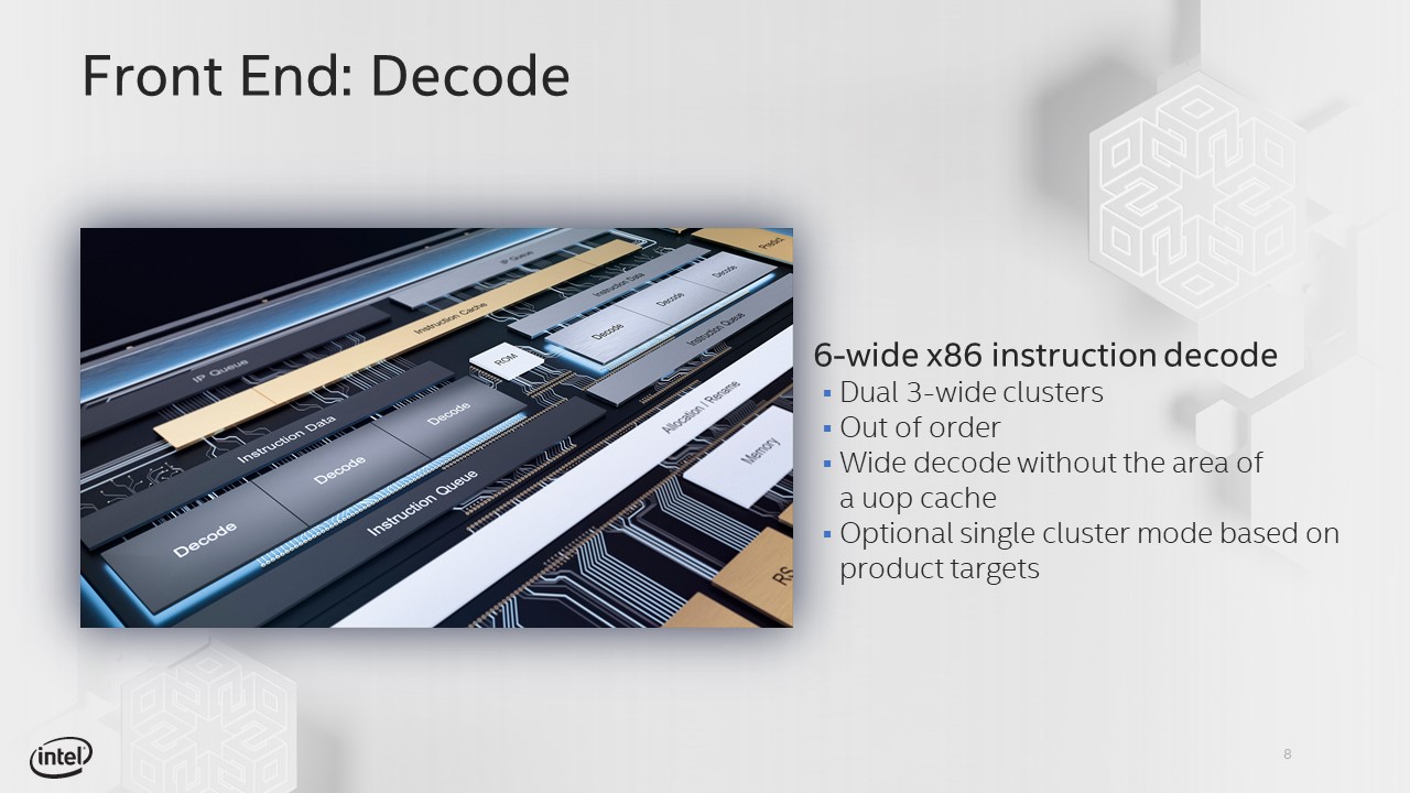
Bits flow into the branch prediction unit (predict), which issues addresses to the Fetch unit, which then loads the instruction cache. This feeds the dual instruction data units that flush to dual 3-wide decode units.
Tremont features path-based prediction on "fairly long" histories, looking for a taken branch on the first 32 bytes of a 64-byte cacheline, but will jump to the second 32 bytes if it can't find a branch in the first half of the cacheline.
The predictor has two levels, with the first being penalty-free, while the larger second-level predictor has a two-cycle penalty. Predictions are handed off to the out-of-order fetch that has a 32KB instruction cache and can issue 32 bytes per cycle.
Decode can process up to six x86 instructions per cycle with two different banks of symmetric complex decoders, meaning all decoders have the capability to process the same instructions. This brings wide native decode capabilities to the architecture without using a micro-op cache, a simplification that equates to die area savings. This also allows the option to run the decoders in parallel, or restricted to save power. The four-wide allocation/rename unit then feeds the integer execution unit.
Intel Tremont Integer and Vector Execution
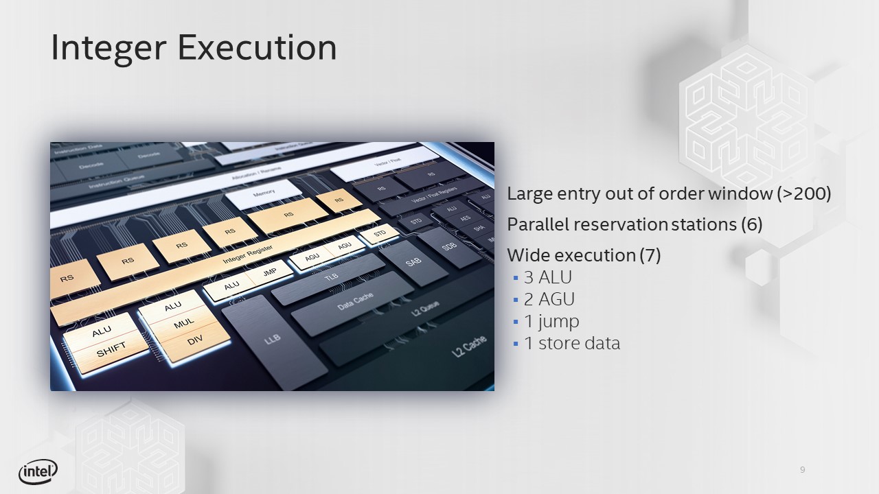
Here we can see the improvements that Intel has made to the integer and vector units. The architecture features a larger 208-entry out of order window to accommodate the increased width, which in turn maximizes parallelism to the execution units. Six reservation stations (most tied to a single end port) feed the three ALU, two AGU (address generation unit), jump, and store ports.
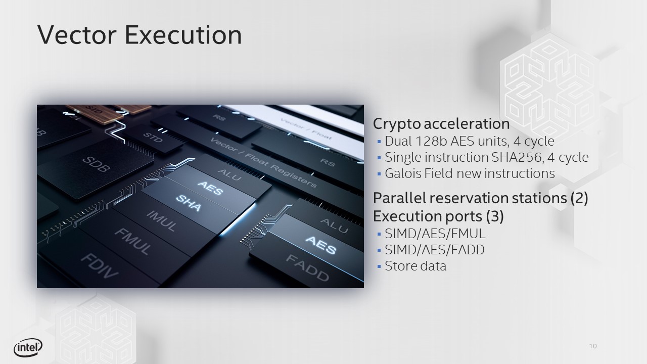
Intel improved crypto-acceleration in the vector unit by integrating dual 128-bit AES units with a four cycle latency, and a single-instruction SHA256 support with a four cycle latency, along with support for new Galois Field instructions.
Vector processing has two SIMD units and two AES units split among two execution ports. Intel also added a floating point multiplier on one of those ports, and an adder on the other port, which allows parallel multiply, add, and store operations.
Intel Tremont Memory Subsystem and New Instructions
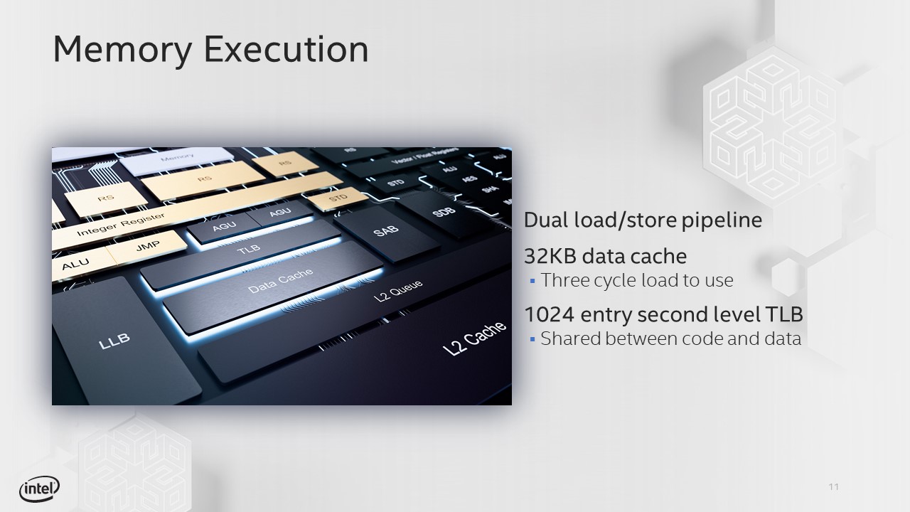
The memory subsystem can dispatch two loads and stores down the pipeline per cycle. The 8-way 32KB data cache has a three cycle load-to-use latency. The five-entry second-level TLB handles requests from both instruction and data cache.
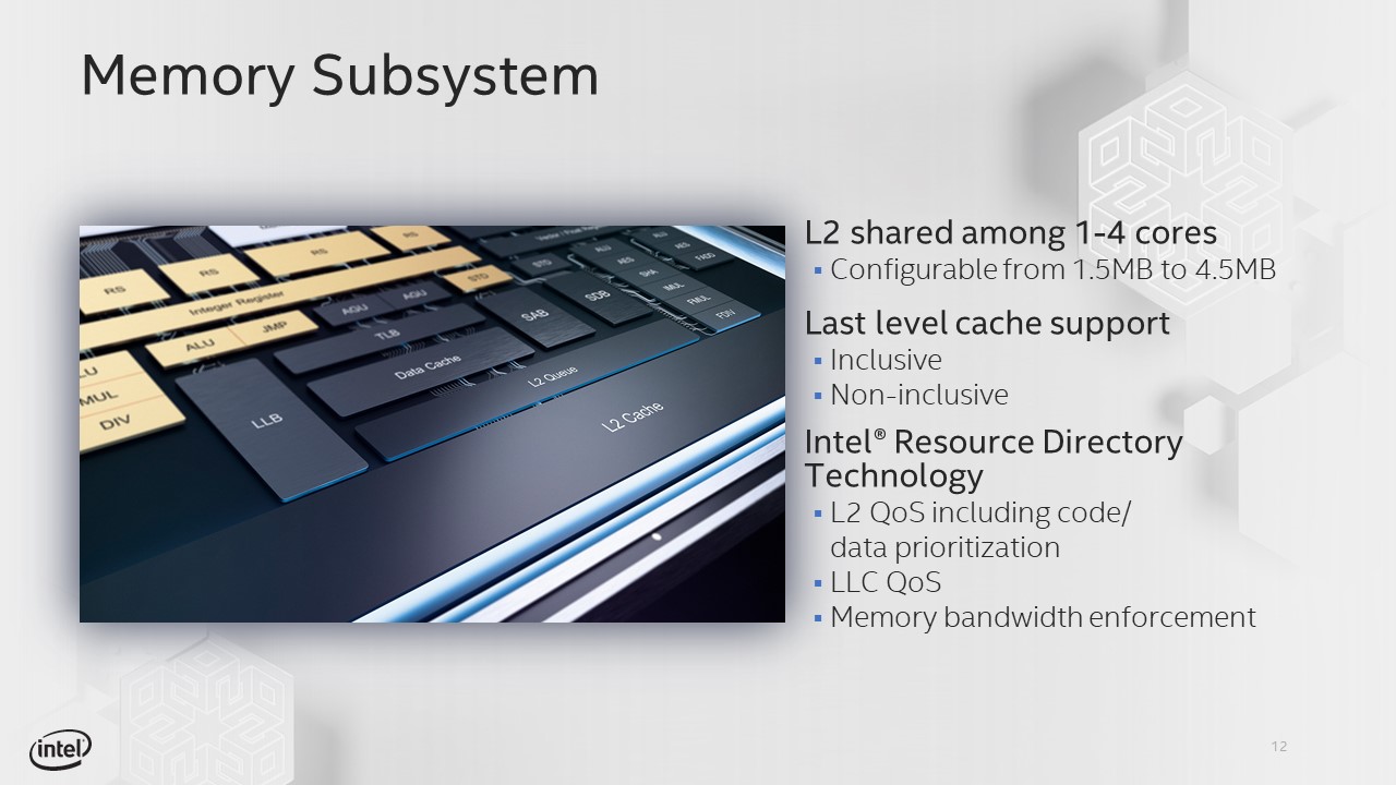
The L2 cache is shared between one to four ports, with 1.5MB to 4.5MB options. Intel also added an L3 cache that can be either inclusive or non-inclusive. The L3 cache enables tying Tremont to other Intel fabrics, like we see with the combination of Sunny Cove and Tremont cores in Lakefield. Intel also added support for Intel Resource Director technology to enable slicing up the cache to enforce fairness or memory bandwidth requirements in either L2 or L3 cache.
Tremont has no specific L3 cache capacity requirements or specifications, instead that is dictated by the particular SoC implementation.
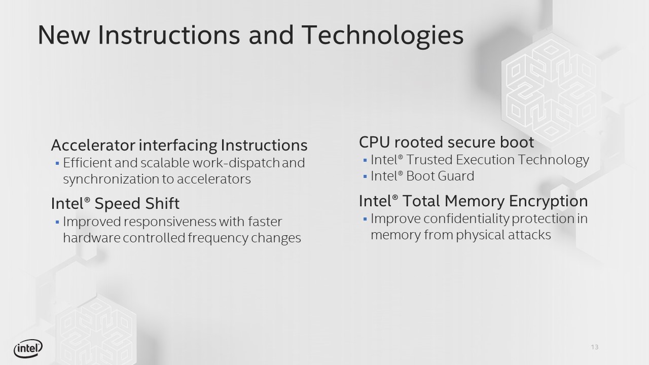
Intel also added new networking- and accelerator-specific instructions, like move-direct instructions that allow traffic optimizations to end points, like the aforementioned networking additives and accelerators. Intel also added secure boot, trusted execution technology, and total memory encryption. Intel also tells us that some of the in-silicon mitigations for recent vulnerabilities have wormed their way into the new silicon, but didn't specify which mitigations are present.
Intel also added Speed Shift technology, which is also present in Kaby and Coffee Lake processors, to speed up power state transitions from idle states by allowing the hardware to control state changes, as opposed to relying upon the operating system to dictate those transitions.
Thoughts
Overall the new Tremont architecture looks impressive and should equate to a new level of performance in the low-power space. However, Intel hasn't shared any detailed plans of forthcoming SoC's with the new cores, so beyond Lakefield, there isn't any indication of when these devices will come to market. We do know that the forthcoming Gemini Lake refresh still uses the Goldmont Plus architecture, so we shouldn't expect Tremont cores to land in that space any time soon.
As we've seen with Intel's 10nm Ice Lake processors, a big jump in IPC doesn't necessarily equate to massive overall performance gains due to the restricted clock speeds of the still-developing 10nm process node. That leaves the jury out on overall performance of the new designs, at least until silicon lands in our labs.

Paul Alcorn is the Editor-in-Chief for Tom's Hardware US. He also writes news and reviews on CPUs, storage, and enterprise hardware.
-
bit_user ReplyAs we've seen with Intel's 10nm Ice Lake processors, a big jump in IPC doesn't necessarily equate to massive overall performance gains due to the restricted clock speeds of the still-developing 10nm process node.
Well, if you're comparing with Gemini Lake, those SoCs were never clocked that high, in the first place.
That leaves the jury out on overall performance of the new designs, at least until silicon lands in our labs.
Realy? You guys are really going to test these SoCs? That's great! I never could get Tom's to touch an Apollo Lake product. -
JayNor Tremont cores are also in Snow Ridge chips.Reply
https://www.tomshardware.com/news/intel-10nm-snow-ridge-tremont-atom-mesh-architecture,40404.html