Intel Details 144-Core Sierra Forest, Granite Rapids Architecture, and Xeon Roadmap
Intel shares P- and E-Core architectures at Hot Chips 2023.
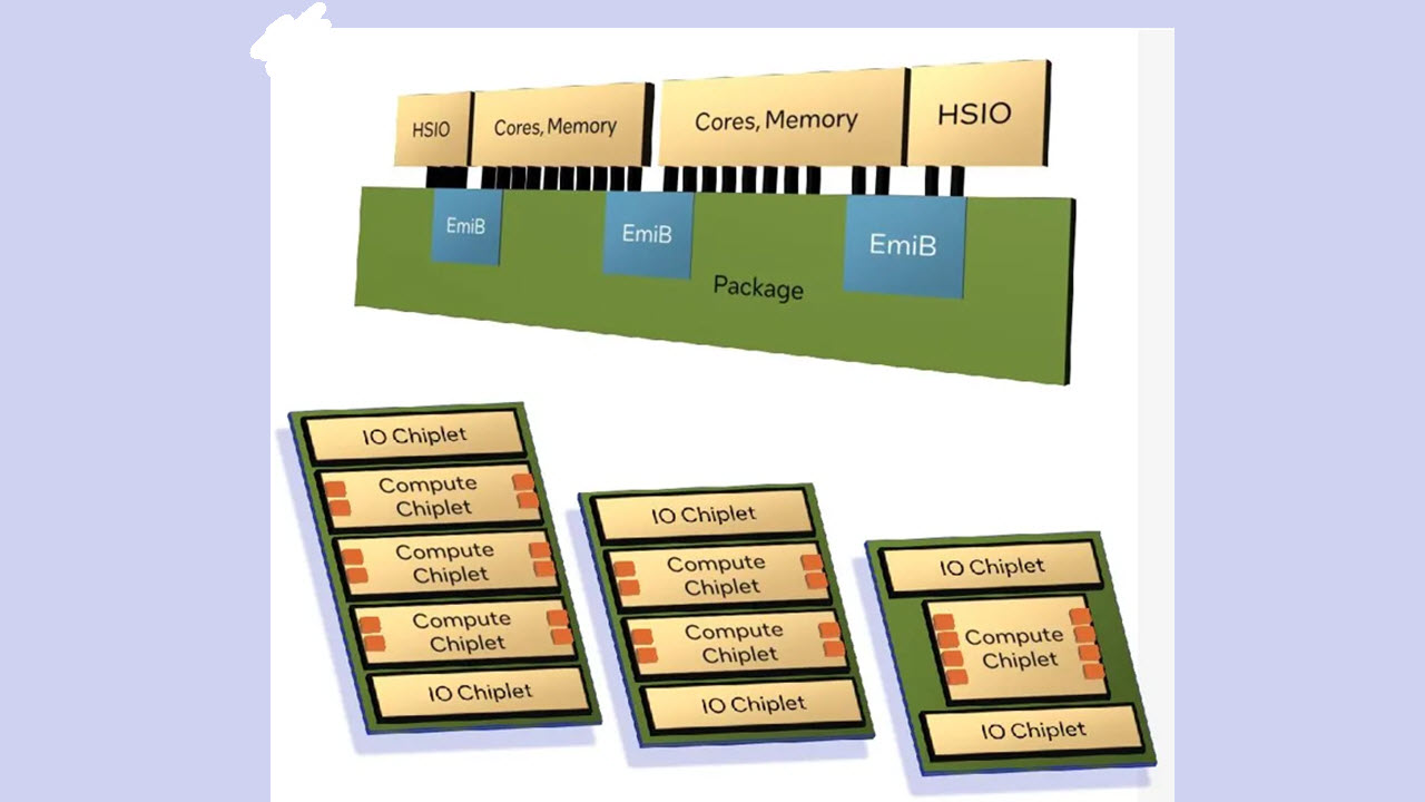
At Hot Chips 2023, Intel unveiled the first deep-dive details of its future 144-core Xeon Sierra Forest and Granite Rapids processors, with the former comprised of Intel's new Sierra Glen E-cores while the latter employs the new Redwood Cove P-cores. The forthcoming next-gen Xeon chips launch in the first half of next year with a new tile-based architecture that features dual I/O chiplets on the 'Intel 7' process paired with varying configurations of compute cores etched on the 'Intel 3' process. This design allows Intel to craft multiple products based on different types of cores while maintaining the same underlying configuration.
Sierra Forest and Granite Rapids drop into the Birch Stream platform with socket, memory, firmware, and I/O compatibility offering a streamlined hardware validation process. They are also interoperable with the same software stacks, thus allowing customers to employ either chip based on their needs.
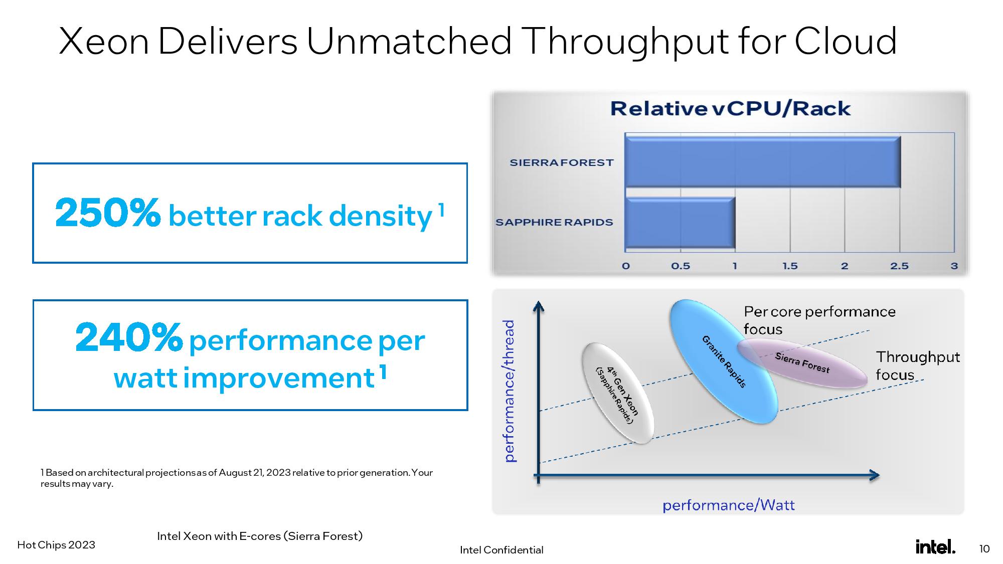
Intel claims the next-gen Xeon Sierra Forest's E-Core-based design will provide up to 2.5x better rack density and 2.4x higher performance per watt than its fourth-gen Xeon chips, while the P-Core powered Granite Rapids will provide 2 to 3x the performance in mixed AI workloads, partially stemming from an 'up to' 2.8X improvement in memory bandwidth. Let's dive in.
Sierra Forest and Granite Rapids Architecture
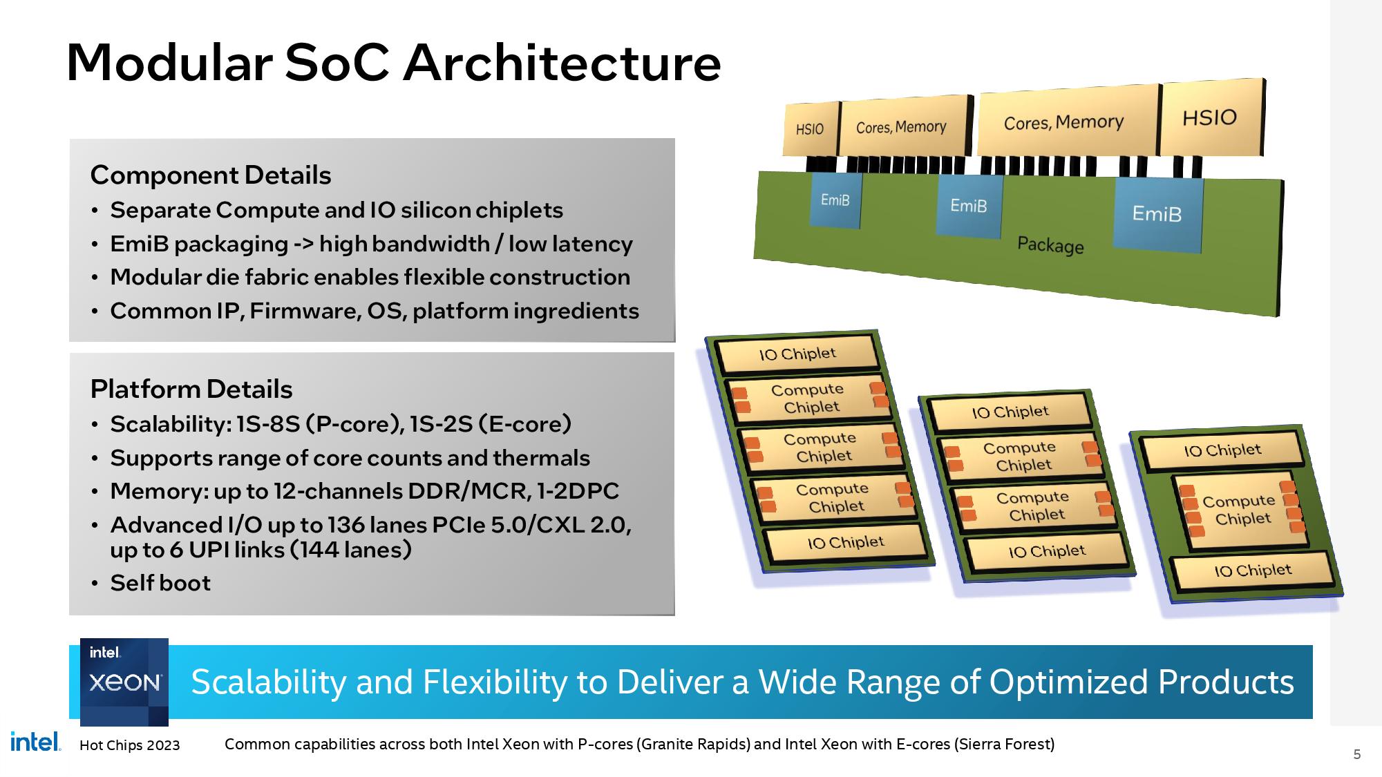
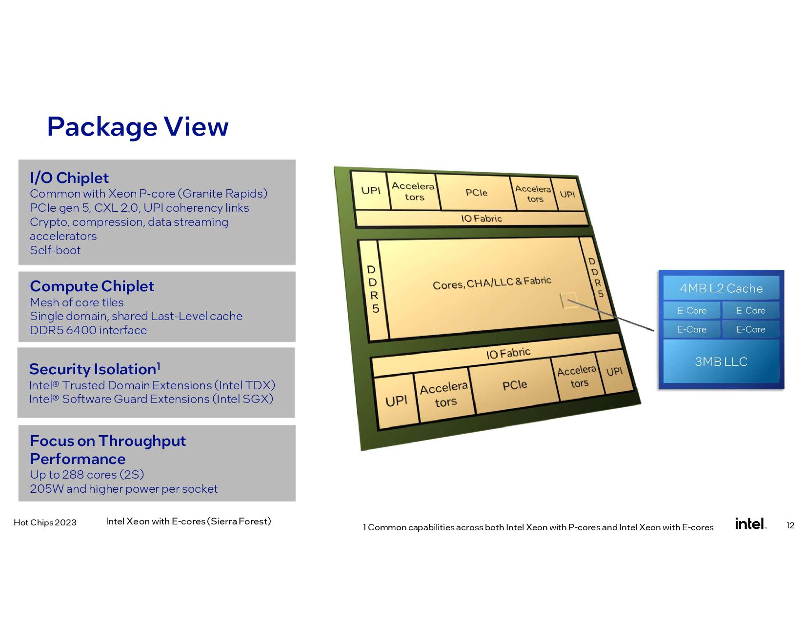
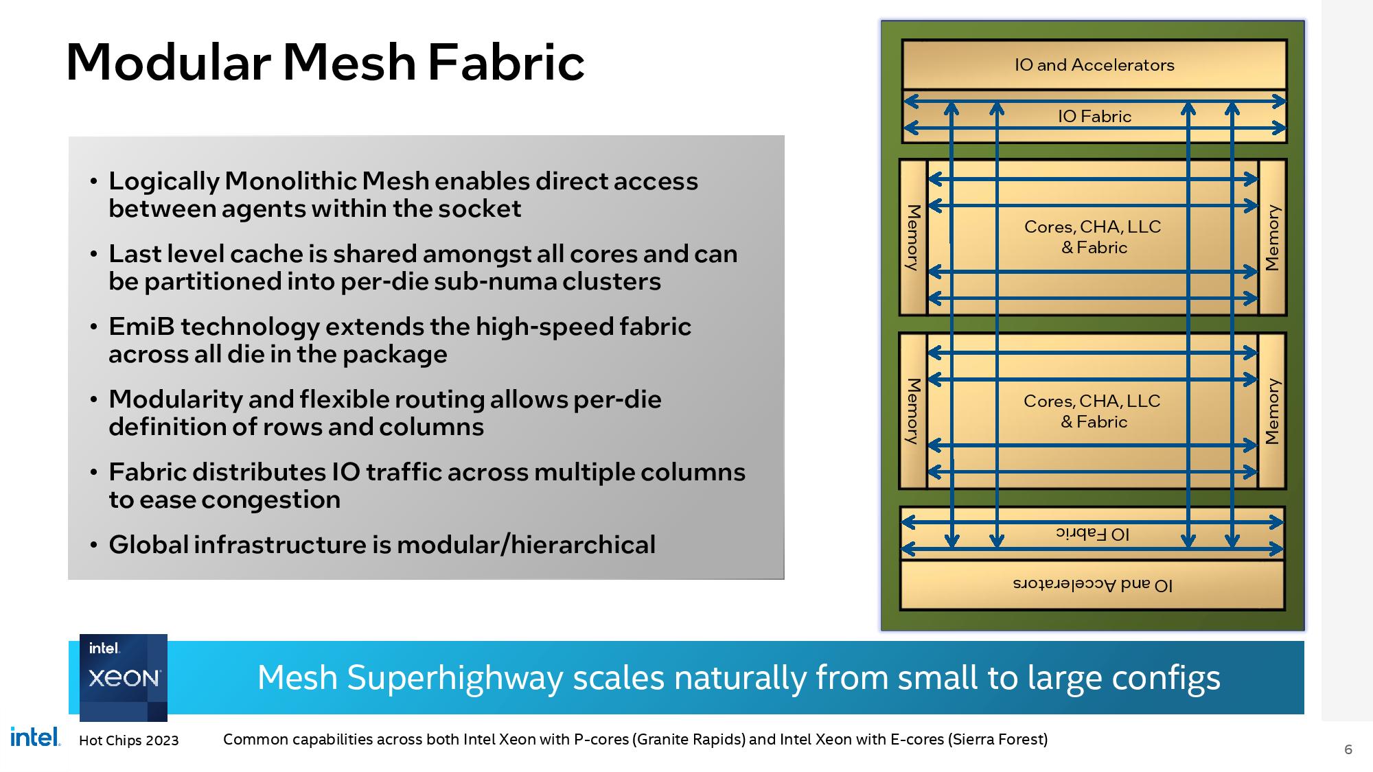
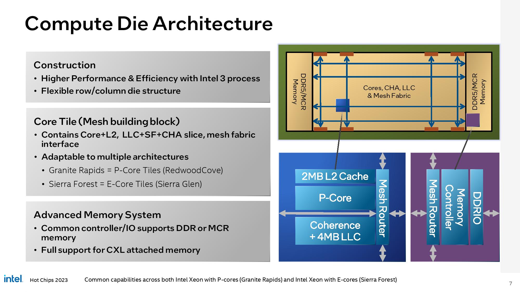
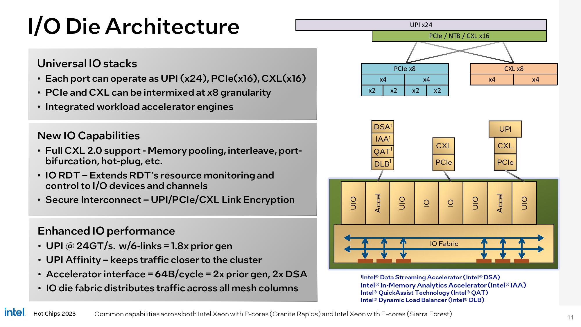
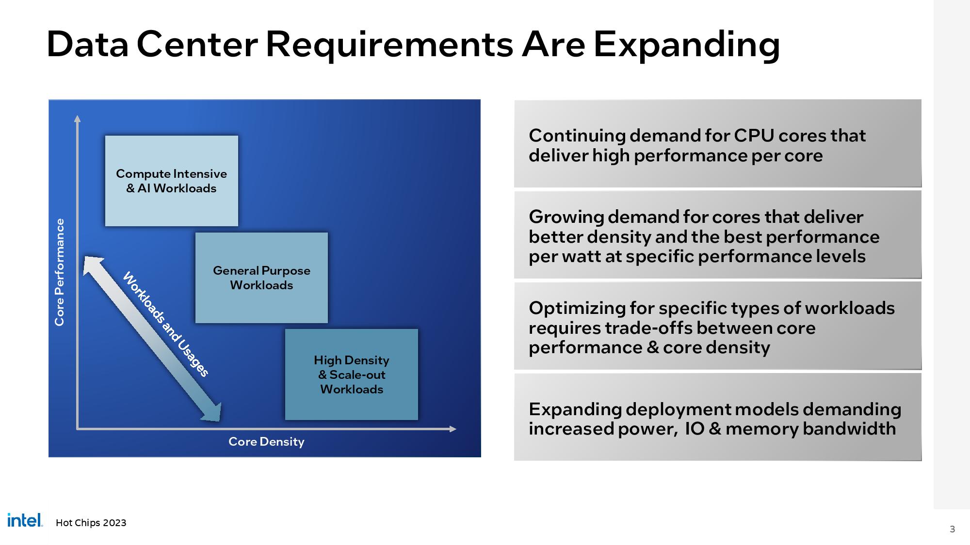
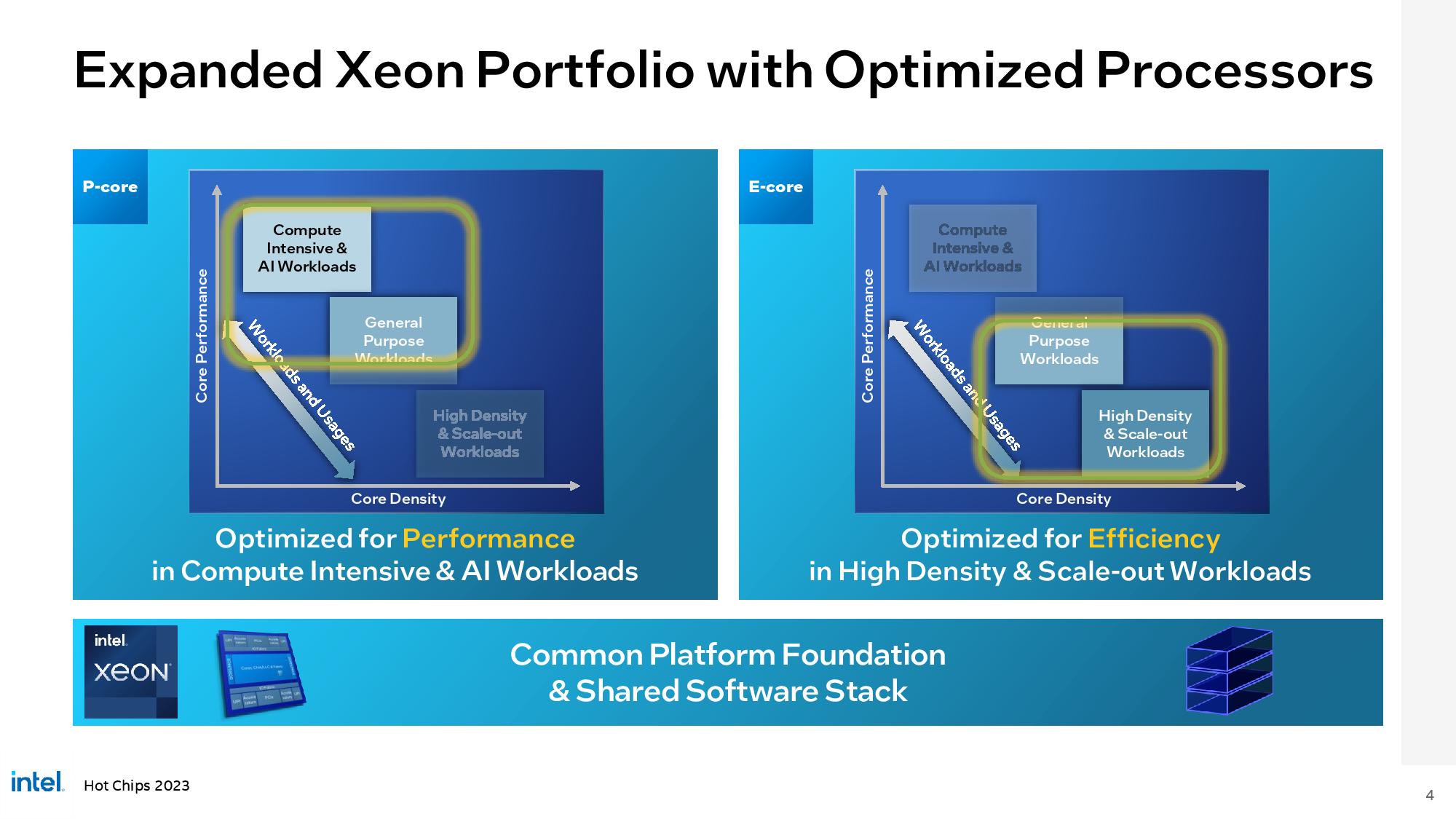
Intel initially moved to a tile-based (chiplet-esque) architecture with its fourth-gen Xeon Sapphire Rapids processors, but Sierra Forest and Granite Rapids bring a new level of disaggregation to the approach.
Intel employed a four-die design with Sapphire Rapids, with each die containing a portion of the relevant I/O functions, like memory and PCIe controllers. The new processors fully disaggregate some I/O functions to two separate HSIO chiplets etched on the Intel 7 process, which offers the best balance of cost, power, and performance for I/O, while the CPU cores and memory controllers reside on their own dedicated compute chiplets.
The two HSIO dies are placed at the top and bottom of the chip package with one to three compute dies in the center, all tied together with an unspecified number of EMIB (Embedded Multi-Die Interconnect Bridge) interconnects fused within the substrate and connected to a die-to-die interconnect at each end of the bridge.
The compute tiles will employ either Redwood Cove P-cores (Performance cores) for Granite Rapids or Sierra Glen E-cores for Sierra Forest — Intel will not provide models with both types of cores in the same package. The compute chiplets come with the EUV-enabled Intel 3 process that features high-density libraries that weren't included with the Intel 4 process and carry 48 P-cores apiece. Intel initially delayed its Granite Rapids Xeons from 2023 to 2024 due to switching the design from 'Intel 4' to 'Intel 3,' but the chips remain on schedule for launch in the first half of 2024.
Granite Rapids is what we would perceive as a traditional Xeon data center processor — these models come equipped with only P-cores that can deliver the full performance of Intel's fastest architectures. Each P-core comes with 2MB of L2 cache and 4MB of L3. Intel hasn't revealed the core counts for Granite Rapids yet but did reveal that the platform supports from one to eight sockets in a single server.
Meanwhile, Sierra Forest's E-core (Efficiency core) lineup consists of chips with only smaller efficiency cores, much like we see with Intel's Alder and Raptor Lake chips, positioning them well to compete with the Arm processors that are becoming more prevalent in the data center. The E-cores are arranged into either two or four-core clusters that share a 4MB L2 cache slice and 3MB of L3 cache. The E-Core-equipped processors come with up to 144 cores and are optimized for the utmost power efficiency, area efficiency, and performance density. Sierra Forest can drop into single- and dual-socket systems and has a TDP 'as low as' 200W.
Regardless of core type, each compute die contains the cores, L2 and L3 cache, and the fabric and caching home agent (CHA). They also house DDR5-6400 memory controllers on each end of the die, with up to 12 channels total (1DPC or 2DPC) of either standard DDR memory, or the new MCR memory that provides 30-40% more memory bandwidth than standard DIMMs.
As you can see above, the compute chiplets will come in different sizes based on the model, with single-compute-die products coming with a larger compute cluster. Intel will also vary the number of memory channels per compute chiplet — here we see three memory controllers on the product with a single compute chiplet, while designs with two or more compute chiplets have two memory controllers apiece. Intel's decision to tightly integrate its memory controllers into the compute chiplet should result in superior memory performance in some workloads compared to AMD's EPYC designs, which employ all of its memory controllers on one central I/O die, thus adding latency and points of contention.
The compute dies share their L3 cache with all other cores in what Intel refers to as a 'logically monolithic mesh,' but they can also be partitioned into sub-NUMA clusters to optimize latency for certain workloads. The mesh ties together the L3 cache slices into a unified shared cache, which can total over half a gigabyte of total capacity — almost 5X larger than Sapphire Rapids. Each die boundary supports over a TB/s of bandwidth between the dies.
Combined, the two HSIO dies support up to 136 lanes of PCIe 5.0/CXL 2.0 (type 1, 2, and 3 devices), up to 6 UPI links (144 lanes), and compression, cryptography, and data streaming accelerators in a similar fashion to Sapphire Rapids' acceleration engines. Each HSIO die also includes power control circuitry that manages the compute chiplets, though each compute chiplet also has its own power control that can operate independently when needed. Intel has now done away with the requirement for a chipset (PCH), thus allowing the processors to be self-booting, much like AMD's EPYC processors.
Intel Sierra Glen E-Core Microarchitecture
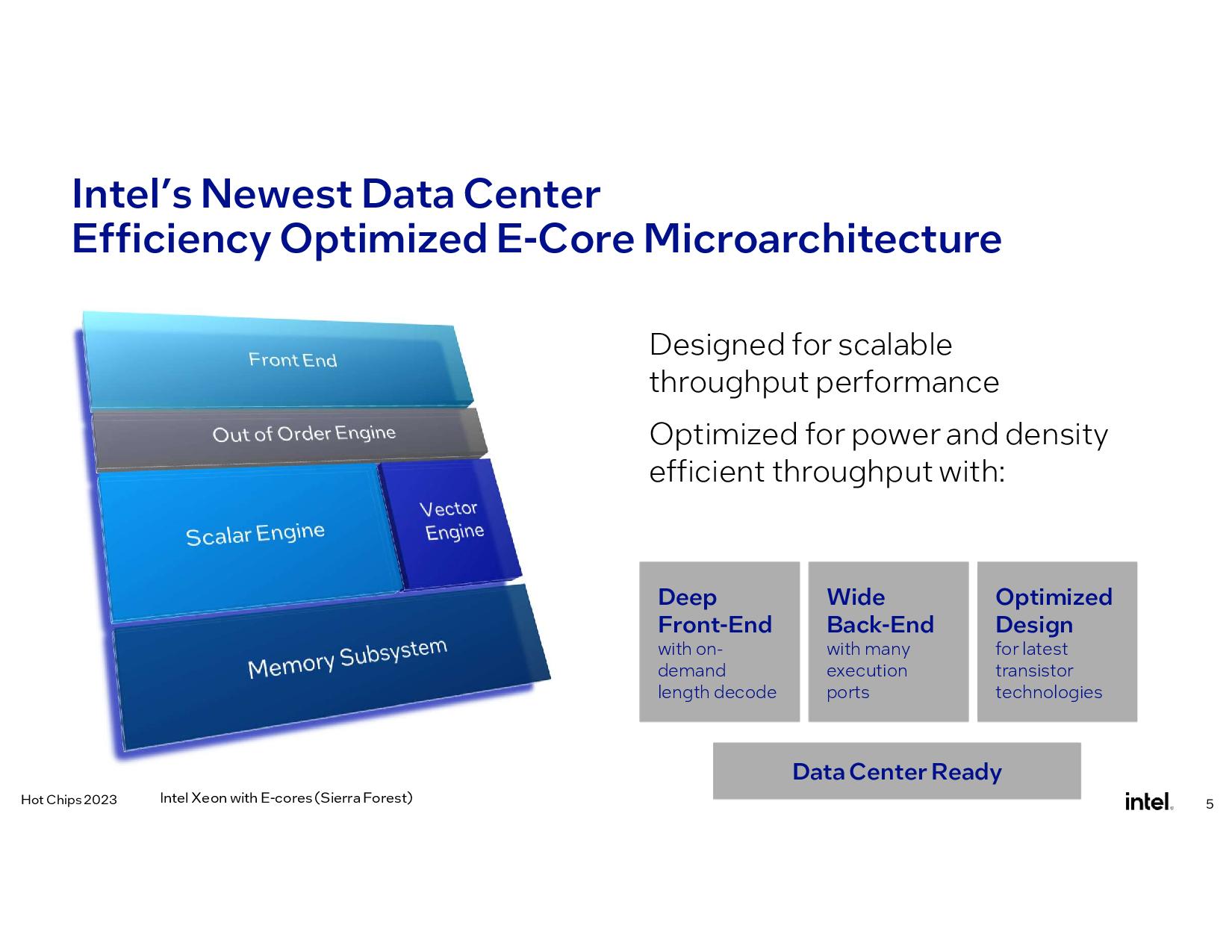
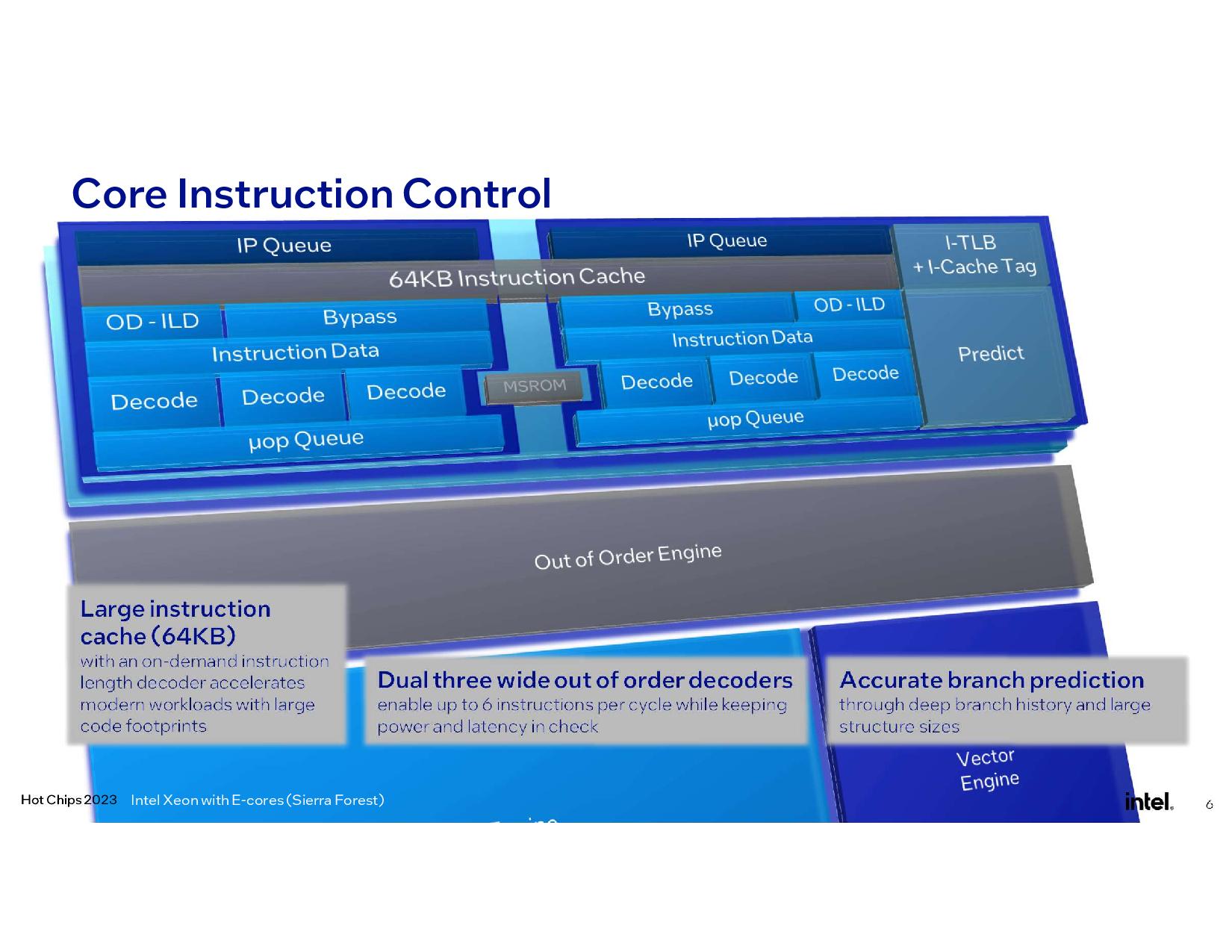
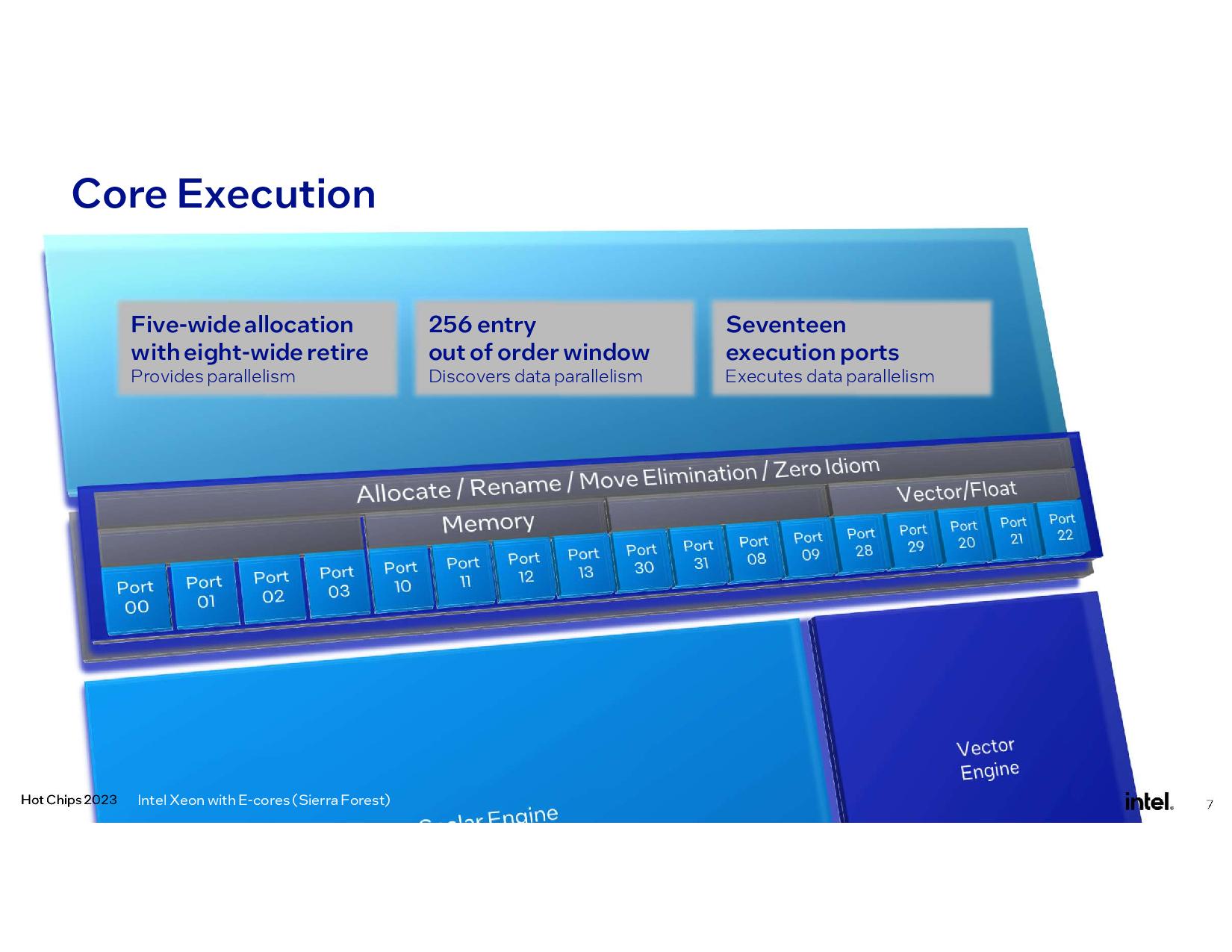
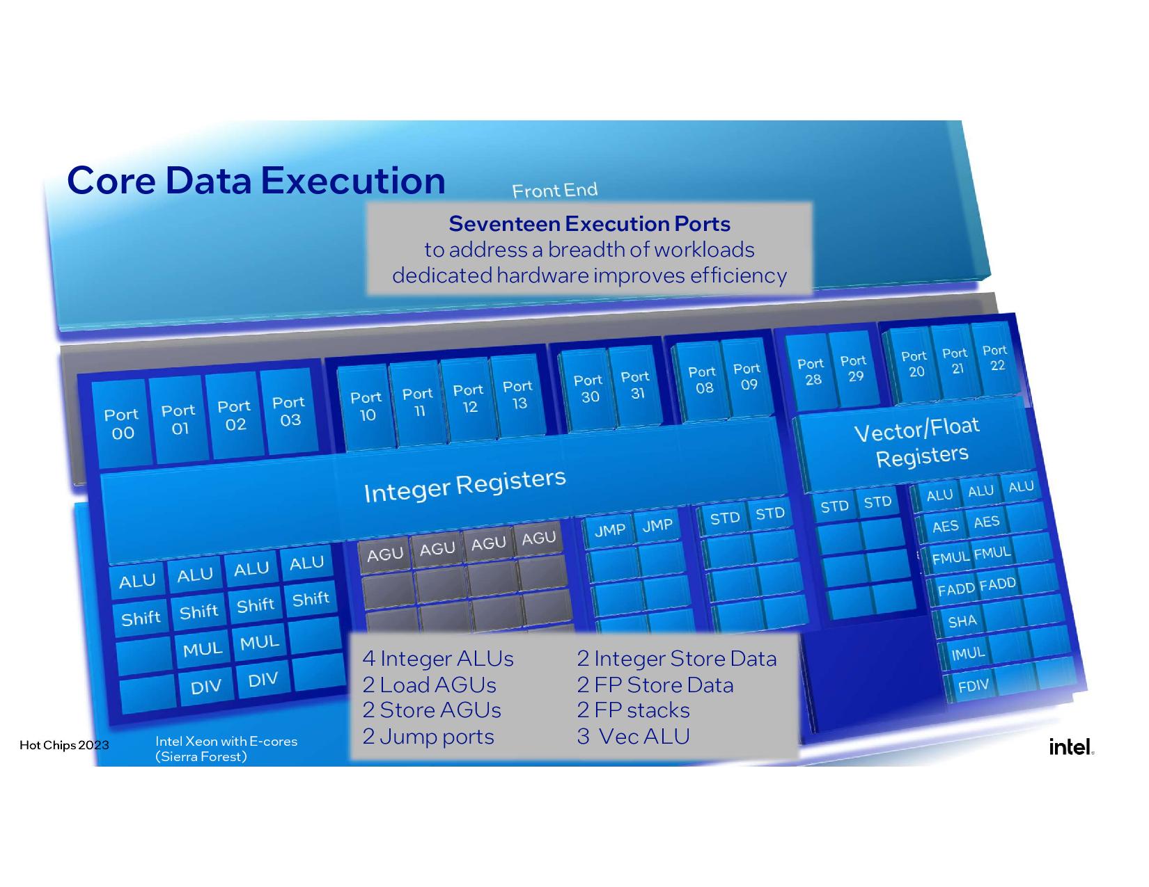
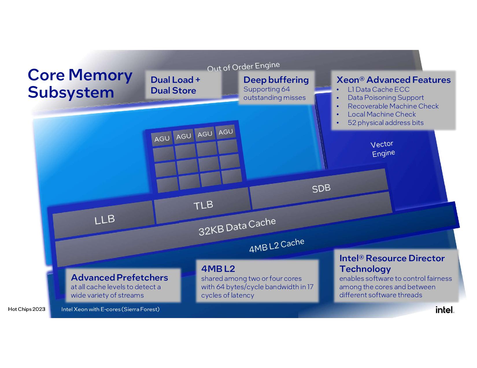
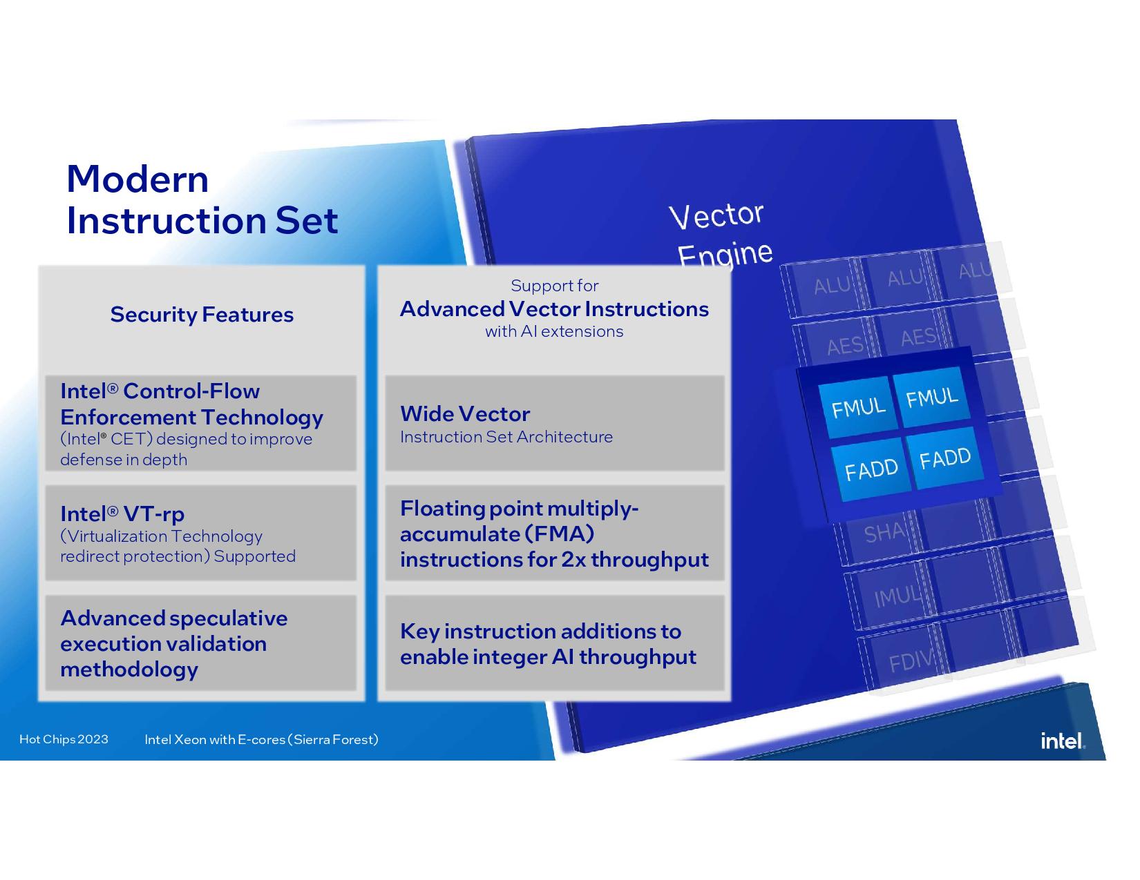
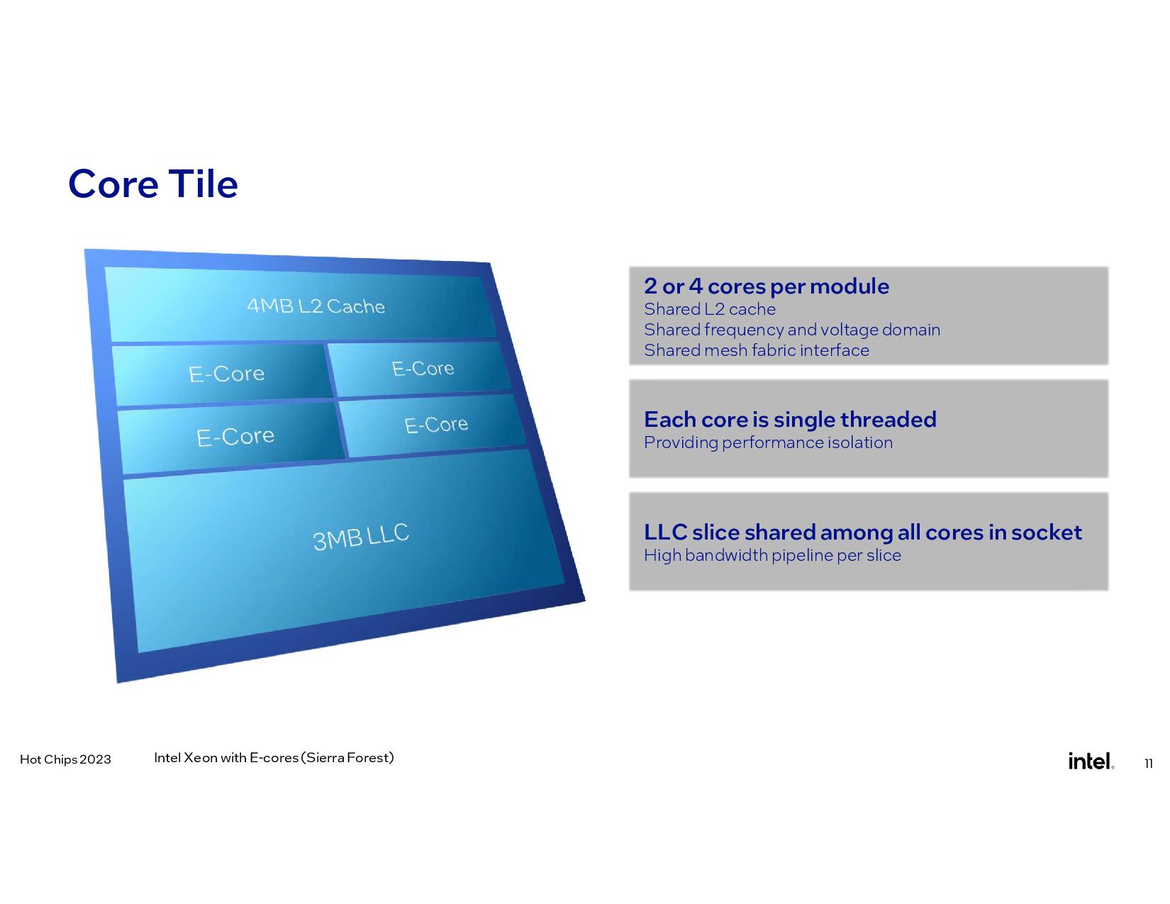
The Sierra Glen microarchitecture is optimized for the best efficiency in scalar throughput workloads, like scale-out, cloud-native, and containerized environments. The architecture features either two- or four-core clusters, allowing Intel to offer certain models with a higher L2 cache capacity per core and more performance per core (via higher power delivery for two-core modules). Each core cluster resides on the same clock and voltage domain. The E-core clusters share a 4MB L2 cache slice and 3MB of shared L3 cache.
As with prior generations, each E-core is single-threaded. Intel also doubled the L1 cache to 64KB and employs a 6-wide decode engine (dual 3-wide to improve latency and power consumption), 5-wide allocate, and 8-wide retire. The Sierra Glen cores do not support AMX or AVX-512, they will rely on AVX10 instead, but Intel did add support for BF16, FP16, AVX-IFMA, and AVX-DOT-PROD-INT8.
Intel Redwood Cove P-Core Microarchitecture
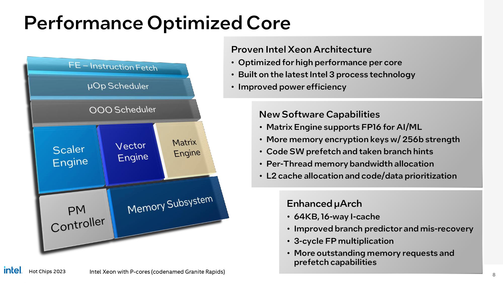
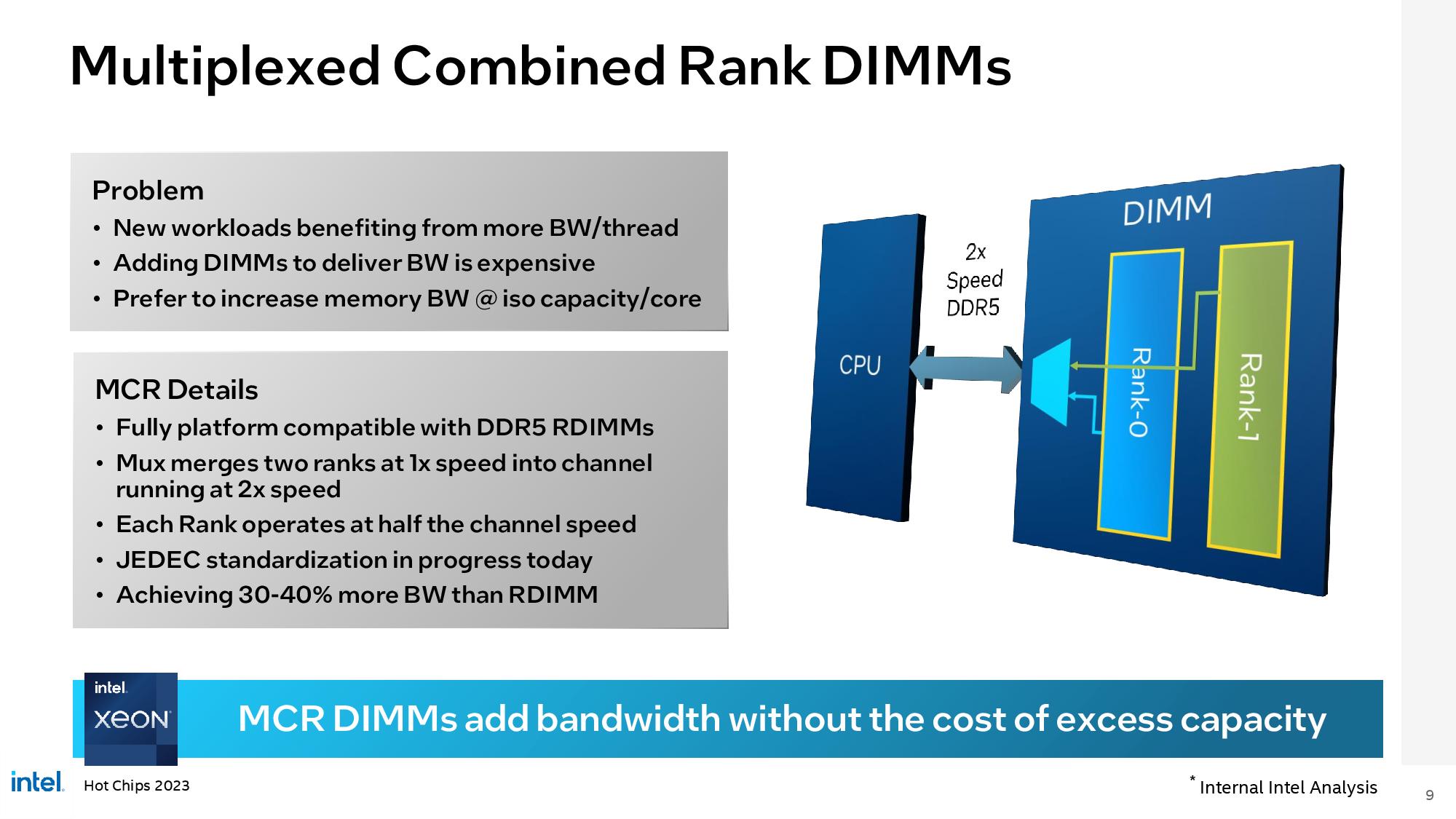
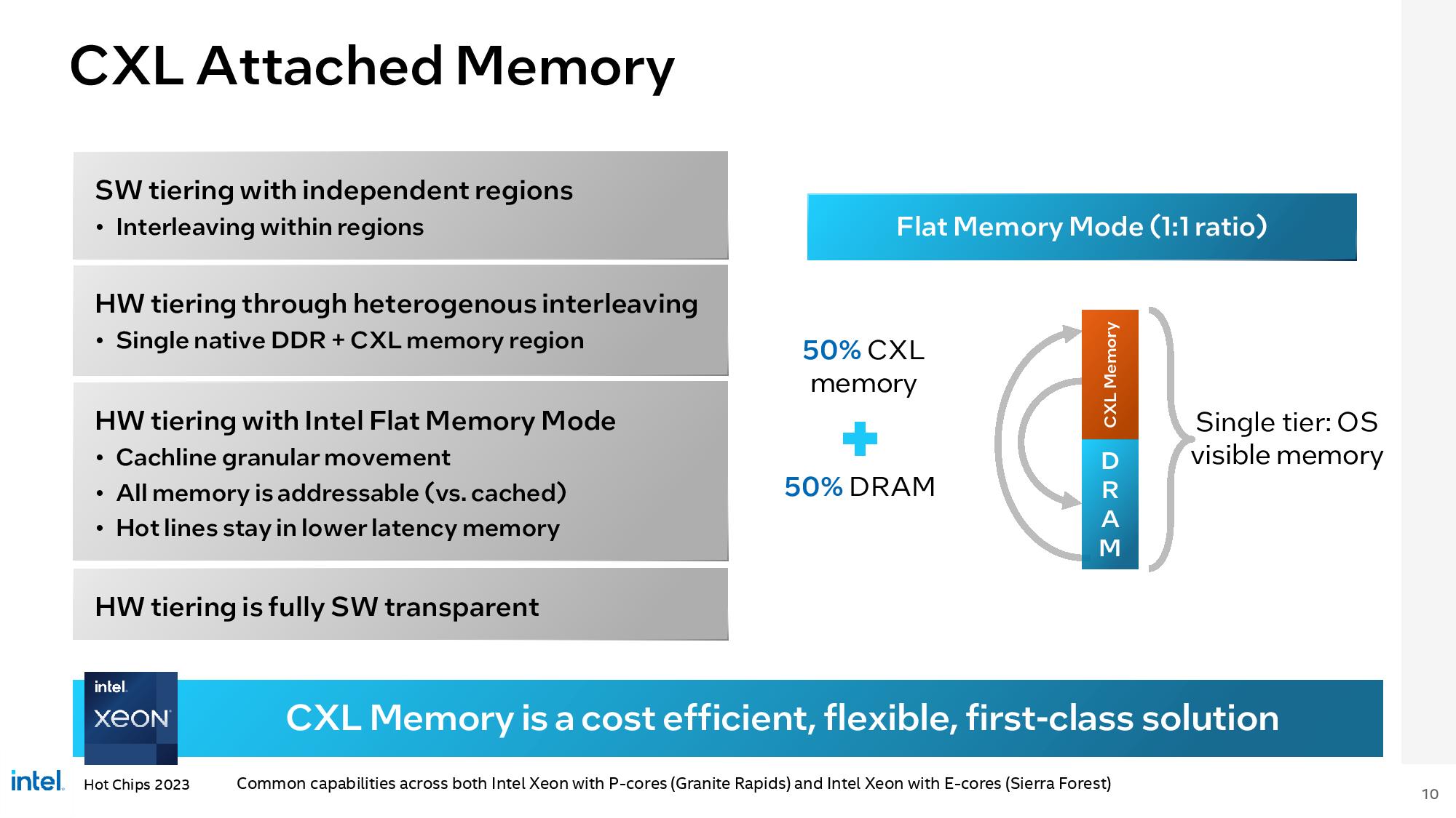
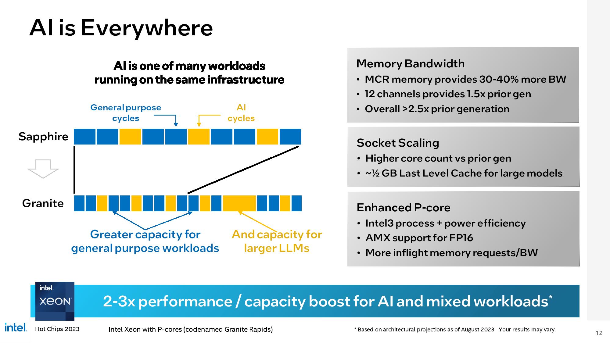
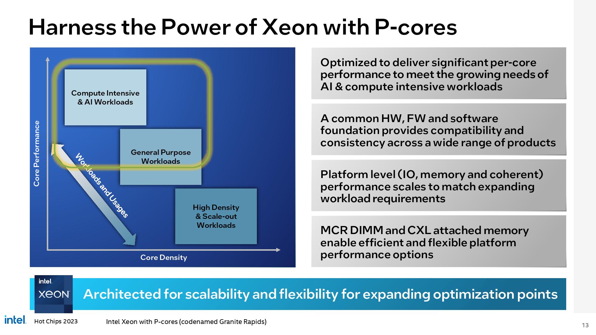
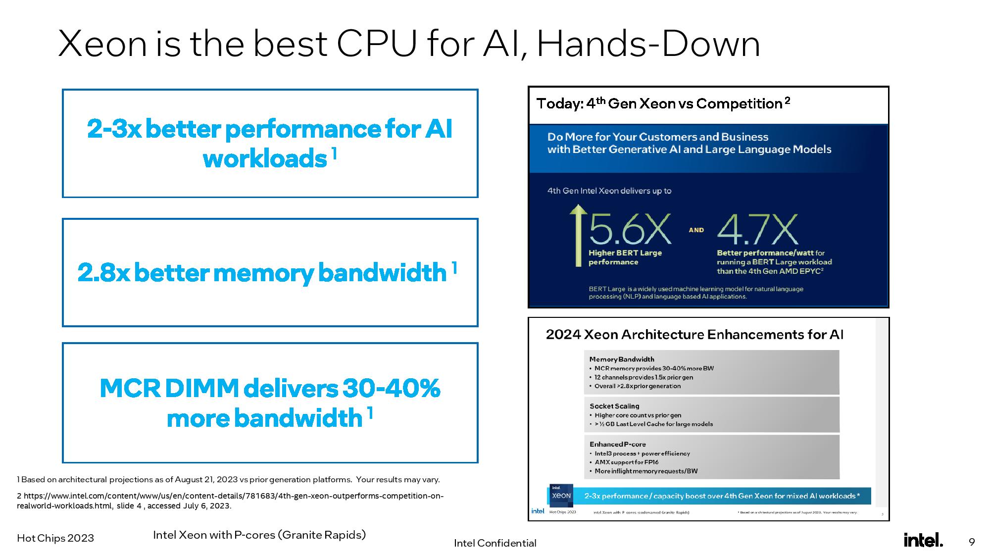
The Redwood Cove architecture for the P-cores now supports AMX with FP16 acceleration, a key addition that will boost performance in AI inference workloads. Intel also doubled the L1 instruction cache capacity to 64 KB to better address code-heavy data center workloads. Redwood Cove also employs software-optimized prefetches and an enhanced branch prediction engine and mis-recovery. Intel also improved floating point performance by moving from 4- and 5-cycle FP operations to 3 cycles, which boosts IPC.
Intel Xeon Roadmap
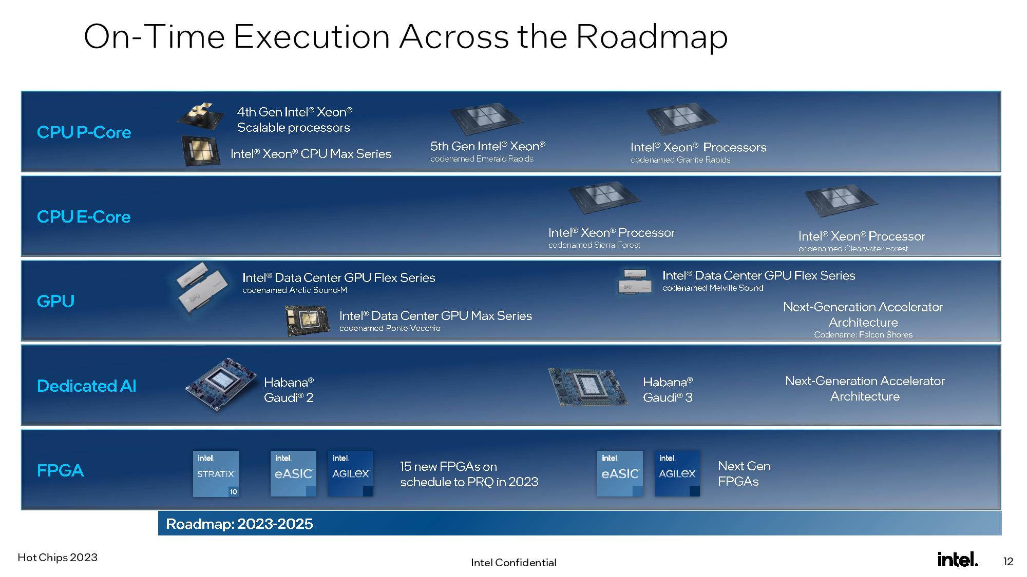
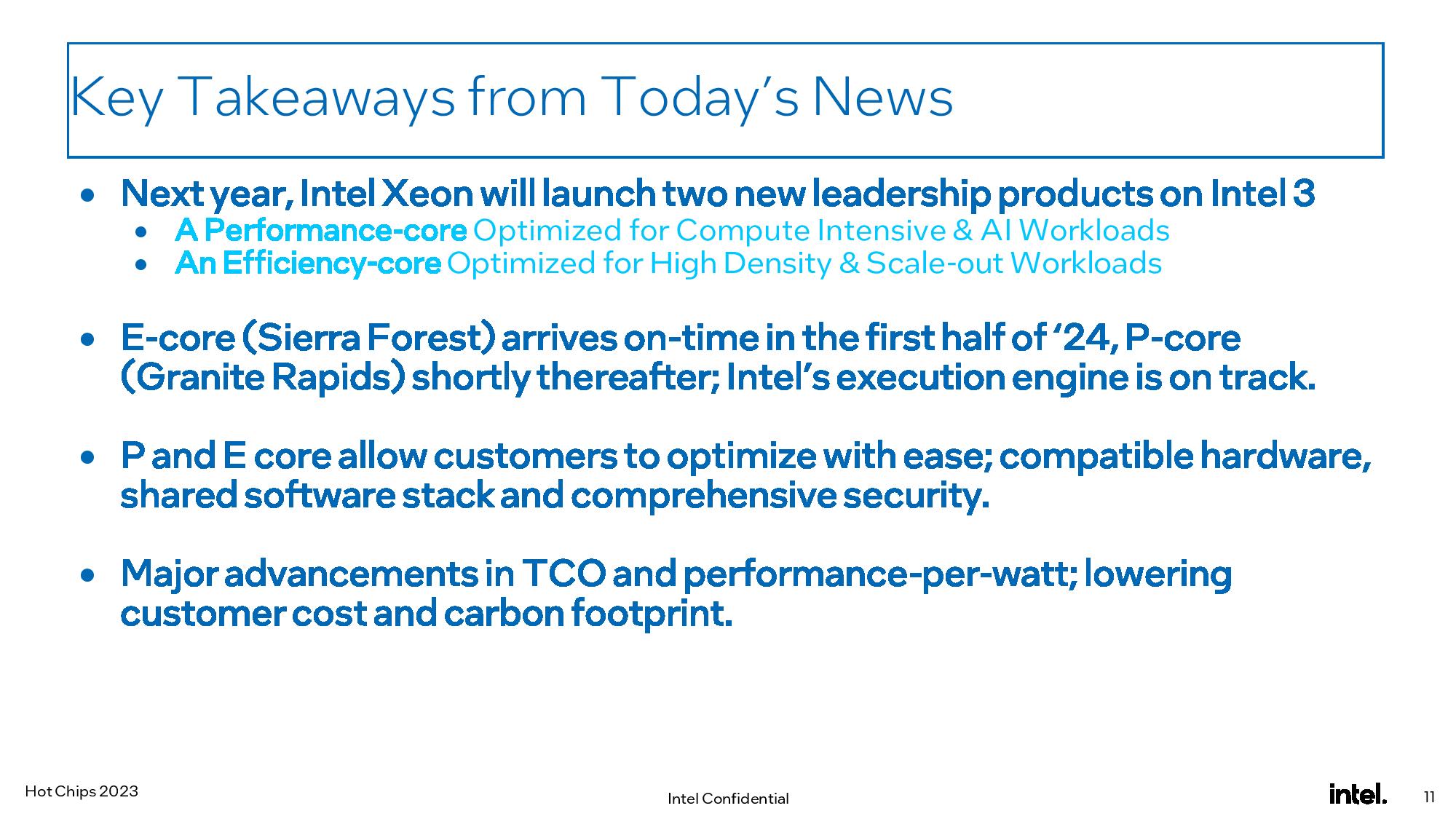
In a bit of good news for Intel, the company's data center roadmap remains on track. Sierra Forest will arrive to market in the first half of 2024, with Granite Rapids following shortly thereafter.
| Row 0 - Cell 0 | 2023 | 2024 | 2025 |
| Intel P-Cores | Emerald Rapids - Intel 7 | Sapphire Rapids HBM | Granite Rapids - Intel 3 | Row 1 - Cell 3 |
| AMD P-Cores | 5nm Genoa-X | Turin - Zen 5 | — |
| Intel E-Cores | — | 1H - Sierra Forest - Intel 3 | Clearwater Forest - Intel 18A |
| AMD E-Cores | 1H - Bergamo - 5nm - 128 Cores | — | — |
Here we can see how Intel’s roadmap looks next to AMD’s data center roadmap. The current high-performance battle rages on between AMD’s EPYC Genoa, launched last year, and Intel’s Sapphire Rapids, launched early this year. Intel has its Emerald Rapids refresh generation coming in Q4 of this year, which the company says will come with more cores and faster clock rates, and it has already released its HBM-infused Xeon Max CPUs. AMD recently released its 5nm Genoa-X products. Next year, Intel’s next-gen Granite Rapids will square off with AMD’s Turin.
In the efficiency swim lane, AMD’s Bergamo takes a very similar core-heavy approach as Sierra Forest by leveraging AMD’s dense Zen 4c cores. Bergamo is already on the market, while Intel’s Sierra Forrest won’t arrive until the first half of 2024. AMD's 5th-gen EPYC Turin chips launch before the end of 2024, but the company hasn't outlined its second-gen Zen 4c model. Intel now has its second-gen E-core-powered Clearwater Forest on the roadmap for 2025.
Get Tom's Hardware's best news and in-depth reviews, straight to your inbox.

Paul Alcorn is the Editor-in-Chief for Tom's Hardware US. He also writes news and reviews on CPUs, storage, and enterprise hardware.
-
dehjomz What’s the difference, if any, between the new Xeon Sierra-Glen E-cores and the new Crestmont E-cores in meteor lake?Reply -
Kamen Rider Blade Given Sapphire Rapids vastly delayed release and it's sketchy availability to average Mom & Pop Small Business retailers, I find Intel's timeline to be vastly optimistic.Reply -
dehjomz Reply
Apparently intel already has the first stepping of arrow lake intel 20a working in the labs. I guess we’ll see if they deliver the new Xeons and the new lakes on time next year.Kamen Rider Blade said:Given Sapphire Rapids vastly delayed release and it's sketchy availability to average Mom & Pop Small Business retailers, I find Intel's timeline to be vastly optimistic. -
Kamen Rider Blade Reply
Hopefully they don't run into as many bugs as Sapphire Rapids has and need so many new steppings.dehjomz said:Apparently intel already has the first stepping of arrow lake intel 20a working in the labs. I guess we’ll see if they deliver the new Xeons and the new lakes on time next year. -
thestryker Reply
I haven't seen anything that indicates there are any differences this go around, but hopefully there will be further clarification. The Xeon E-cores are going to be available in a 2 core cluster which I imagine the consumer chip versions will not.dehjomz said:What’s the difference, if any, between the new Xeon Sierra-Glen E-cores and the new Crestmont E-cores in meteor lake? -
bit_user Reply
This is just a wild guess, but I wonder if the main difference isn't the process node. Meteor Lake is being made on Intel 4, while Sierra Forest will be made on Intel 3. I can't think of an example where Intel changed the process node and didn't also call the core something different.dehjomz said:What’s the difference, if any, between the new Xeon Sierra-Glen E-cores and the new Crestmont E-cores in meteor lake?
Their slide on that suggest they achieve this by simply disabling two of the four. Perhaps the ability to have partially-disabled clusters was done for yield reasons?thestryker said:The Xeon E-cores are going to be available in a 2 core cluster which I imagine the consumer chip versions will not.
It's certainly possible that Arrow Lake could adopt the same technique. That would scale down much better, if you could reduce E-core count by de-populating the cores within clusters, rather than having to switch off entire clusters. -
DaveLTX Intel already has memory controllers on the same chiplet as the CPU cores but unfortunately inter mesh communication isn't good.Reply
Meshes just aren't great at latency, as compared to AMD's chiplets that uses ring buses
And besides, VM workloads reside on the private chiplet caches or out to DRAM, not go looking for caches in other cores. -
bit_user Also, it looks like they're going after CXL, in a big way. This is just one of several slides to mention it, but I thought it had the most interesting details.Reply
-
thestryker Reply
They also spoke of the E-core based Xeons having a full list of SKUs instead of just high core count. It's possible this is just how they're doing lower core count models while using the same die across every SKU.bit_user said:Their slide on that suggest they achieve this by simply disabling two of the four. Perhaps the ability to have partially-disabled clusters was done for yield reasons? -
bit_user Reply
The last server CPU Anandtech reviewed was Ice Lake, however it gives us a chance to compare a fairly recent mesh vs. Milan (Zen 3)'s interconnect topology.DaveLTX said:Intel already has memory controllers on the same chiplet as the CPU cores but unfortunately inter mesh communication isn't good.
Meshes just aren't great at latency, as compared to AMD's chiplets that uses ring buses
If you click on these images and look at the numbers written in the cells, you can see that core-to-core communication latency is markedly better in Ice Lake.
Ice Lake SP 8380
EPYC Milan 7763
Now, here's how they compare on memory latency:
Ice Lake SP 8380
EPYC Milan 7763
Source: https://www.anandtech.com/show/16594/intel-3rd-gen-xeon-scalable-review/4
DRAM latency is definitely better in Ice Lake. Furthermore, in spite of having much more L3 cache, overall, Milan blows out of it sooner. That's because a chiplet can only populate its local L3 slice.
The point of Intel's shared L3 approach is that you can get more flexible sharing of L3 across the cores. In the best case, that could enable you to get more benefit from the same amount of L3 as in EPYC.DaveLTX said:And besides, VM workloads reside on the private chiplet caches or out to DRAM, not go looking for caches in other cores.
As for the part about "looking for caches in other cores", cache-coherency demands that all caches be checked, when you have a cache miss in a given slice of L3.