Micron's New HBM3 Gen2 is World's Fastest at 1.2 TB/s, Teases Next-Gen at 2 TB/s+
Fastest, densest and most power efficient yet.
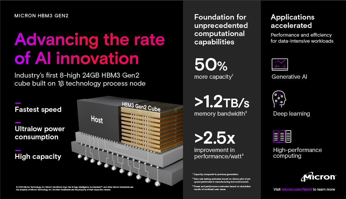
Today Micron announced its new HBM3 Gen2 memory is sampling to its customers, claiming it's the world's fastest with 1.2 TB/s of aggregate bandwidth and the highest-capacity 8-high stack at 24GB (36GB is coming). Micron also claims its new memory is the most power efficient, with a 2.5x improvement-per-watt compared to the company's previous-gen HBM2E. Micron's HBM3 Gen2 also has a 12-high stack option that totals 36GB that's coming 'soon.'
Micron is the first to sample what it terms second-gen HBM3 memory, outstripping rivals like SK hynix and Samsung, which could be an advantage given the current AI arms race that finds vendors scrambling for the fastest and most capacious memory possible to power memory-hungry AI accelerators.
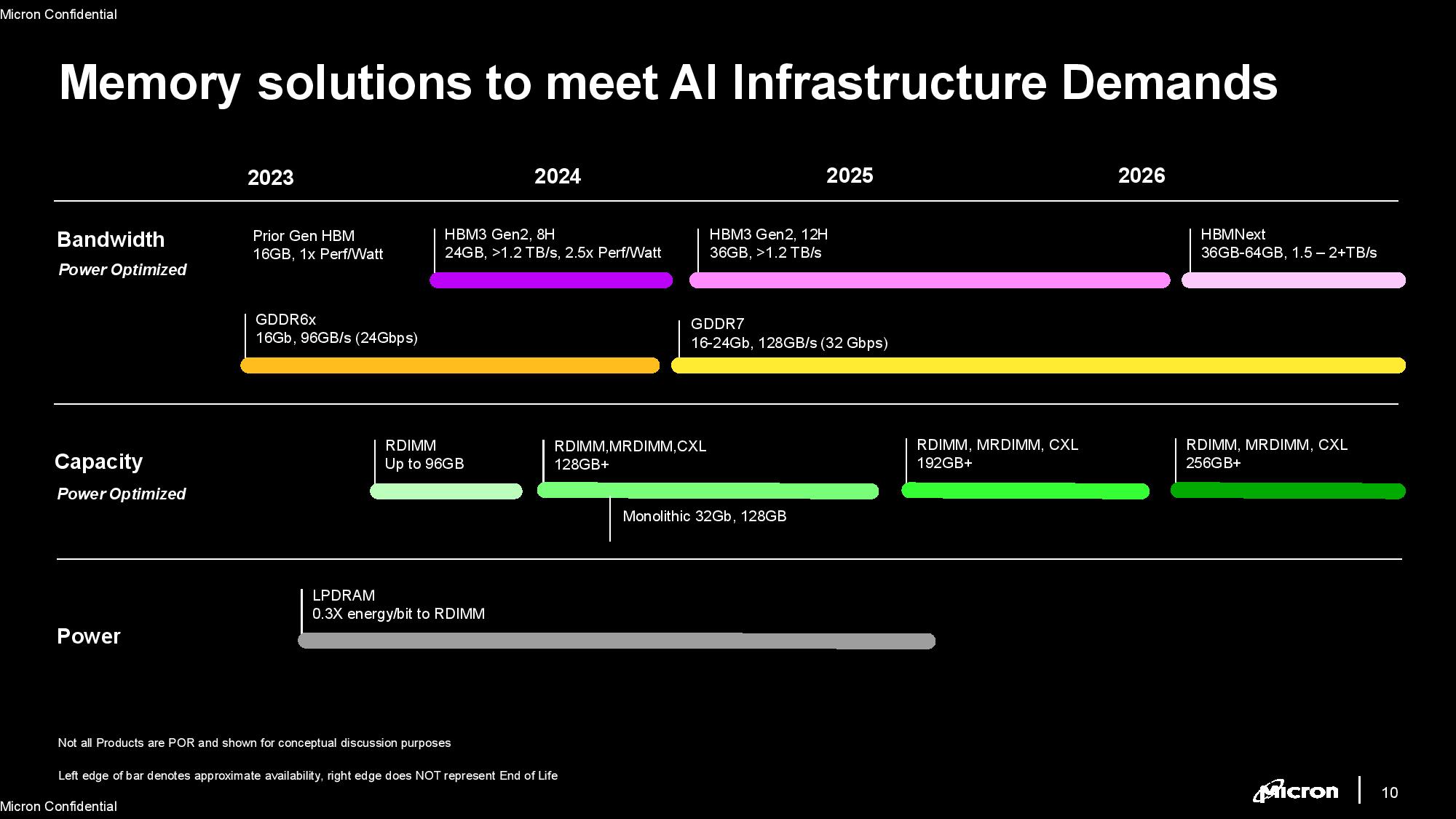
Micron's HMB3 Gen2 offers the highest bandwidth of its memory portfolio. Micron has essentially skipped over releasing a standard HBM3 offering, moving from HBM2E to its 'HBM3 Gen2.' Micron says the new 'Gen2' naming convention is to 'represent the generational leap in performance, capacity, and power efficiency.'
We can also see an 'HBMNext' listed on Micron's roadmap, which could be HBM4. This next-gen memory will deliver 2+ TB/s of throughput and up to 64GB of capacity when it arrives ~2026.

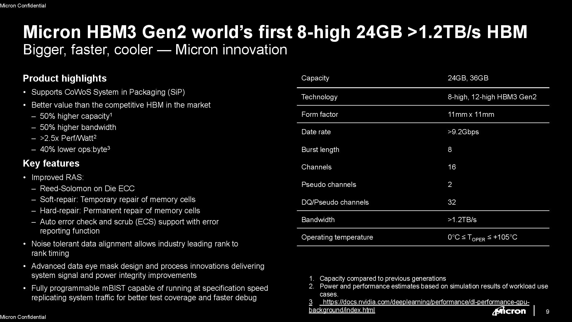
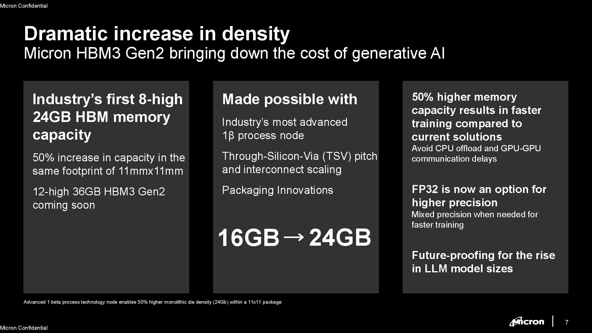


Micron's new HBM3 Gen2 memory has eight stacked 24Gb die (8-high) that provides a 50% capacity increase over other 8-high HBM3 stacks — HBM3 currently tops out at 24GB with a 12-high stack. Micron's new memory also fits into the same 11mmx11mm footprint as standard HBM3, marking a significant density increase. The package is drop-in pin compatible with existing HBM3, making it a relatively easy task to swap in the faster memory.
Micron's HBM3 Gen2 also has a 12-high stack that totals 36GB that's coming 'soon.' For a device with eight HBM packages like AMD's MI300, that would enable up to 288 GB of capacity, while the more-common 6 stacks, like we see with Nvidia's H100, would equate to 216 GB of capacity.
The 8-high stack delivers 50% higher bandwidth with 9.2 Gbps per pin, which works out to 1.2 TB/s with a 1024-bit wide memory bus. That's 50% faster per pin than current HBM3 memory, which tops out at 6.4 Gbps per pin and 820 GB/s of aggregate throughput. Naturally, performance will scale with larger memory subsystems.
| Row 0 - Cell 0 | Micron HBM3 Gen2 | HBM3 | HBM2E | HBM2 |
Maximum Capacity | 24 | 36 GB | 16 GB | 24 GB | 16 GB | 8 GB |
Stack Height | 8-high | 12-high | 8-high | 12-high | 8-high | 12-high | 8-high |
Bandwidth Per Pin | 9.2 Gbps | 6.4 Gb/s | 3.6 Gb/s | 2 Gb/s |
Total Bandwidth | 1.2 TB/s | 819 Gb/s | 460 GB/s | 256 GB/s |
Bus Width | 1024-bit | 1024-bit | 1024-bit | 1024-bit |
Voltage | 1.1V | 1.1V | 1.2V | 1.2V |
It's natural to expect that HBM3 Gen2's higher capacity and bandwidth will result in higher heat, but Micron took several steps to improve thermals to defray potential issues. Micron uses the same 1β (1-beta) process node for HBM3 Gen2 as it uses for its current-gen DDR5 memory. This node, which is Micron's last non-EUV DRAM node, brings with it both density and power efficiency improvements over the memory used for its standard HBM3.
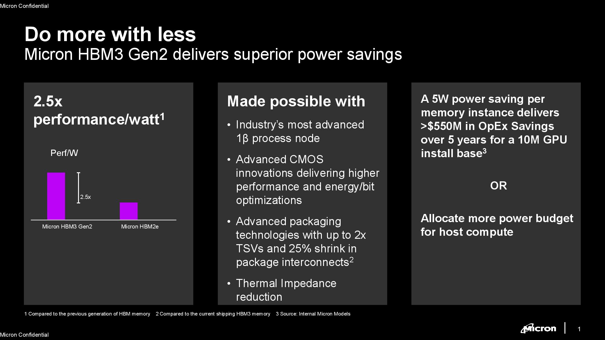
Micron claims that its HBM3 Gen2 delivers a 2.5x improvement in performance-per-watt over its prior-gen HBM2E, and a >50% improvement in Pj/bit (picojoules a bit) over the previous generation (Micron declined to provide a specific number).
Micron reduced the space between the individual DRAM layers by 23%, which helps thermal transfer from the lowest die (which tends to be the hottest) to the top die (which tends to be the coolest). The air between the layers can also have an insulative effect, so reducing the distance between the die has the knock-on effect of reducing the air gap. However, Micron still adheres to the standard 720um Z-height (thickness) of the final package.
Micron also doubled the number of TSVs, which helps improve power efficiency due to increased data lanes, and shrunk the interconnects by 25% compared to current-gen HBM3 (the company declined to share the pitch). The denser metal TSV interconnects also help improve thermal transfer between the layers of the device. Micron also says its HBM3 Gen2 has "a five-time increase in metal density," which also reduces thermal impedance. In culmination, the package fits within the standard 0C to 105C operating range despite the increased capacity and throughput.
Micron says its HBM3 Gen2 has a noise-tolerant design and features advanced signal and power integrity, though Reed-Solomon on Die ECC (error correction code) steps in to correct any issues. Since this is on-die, an extra die isn't required for ECC.
Micron's HBM3 Gen2 package is compatible with standard CoWoS packaging; a must given the industry's preference for this type of packaging for GPUs and other types of accelerators. The HBM3 Gen2 memory has the same channel arrangement as HBM3, with 16 channels and 32 virtual channels (two pseudo-channels per channel).
Micron is the first to ship samples of a second-gen HBM3, but SK hynix recently revealed that it has 24GB HBM3E stacks under development for release in 2024. However, those products are said to peak at 8 Gbps per pin (1TB/s in aggregate), which would give Micron a ~20% advantage in overall bandwidth. Naturally, we'll have to wait for a final announcement from SK hynix before making a more thorough comparison.
Micron's HBM3 Gen2 is sampling to partners now for 8-high stacks, and 12-high stacks will arrive in the near future. High volume production begins in 2024.
Get Tom's Hardware's best news and in-depth reviews, straight to your inbox.

Paul Alcorn is the Editor-in-Chief for Tom's Hardware US. He also writes news and reviews on CPUs, storage, and enterprise hardware.
-
bit_user ReplyThe HBM3 Gen 2 memory has the same channel arrangement as HBM3, with 16 channels and 32 virtual channels (two pseudo-channels per channel).
So, does anyone know what this actually means? Is it like DDR5, where you have 2x 32-bit channels per DIMM, or is it more like you have two virtual channels interleaved over each real 64-bit channel?
Also, is HBM typically interleaved? If so, at what granularity? -
Diogene7 ReplyAdmin said:Micron announced that its HBM3 Gen 2 memory, which is the Fastest, densest and most power efficient yet, is now sampling to its partners.
Micron's New HBM3 Gen2 is World's Fastest at 1.2 TB/s, Teases Next-Gen at 2 TB/s+ : Read more
I am wondering how much more energy efficient per bit HBM3 is compared to LPDDR5 ? And also how much more expensive it is at iso-capacity (ex: In July 2023, let say that 32GB LPDDR5 6400 cost 100$ to 150$, (fictious numbers) how much would be 32GB HBM3 6400 ?)
Why don’t we have such technology in smartphones and laptops ? One or two 32GB stacks would provide lot of memory and bandwith to the CPU…
Also what would be a disruptive innovation / improvement is to have 32GB or more low power consumption non-volatile (VCMA) MRAM HBM stack: in theory, it could be used to replace LPDDR DRAM memory and NAND Flash storage, with very fast non-volatile memory in one device : most software actions would likely feel near instantaneous (no or less loading time), with nearly no need for time to boot the system (« instant-on »). -
bit_user Reply
Nvidia addressed some of these questions in their justification for choosing LPDDR5X for use with their Grace CPU:Diogene7 said:I am wondering how much more energy efficient per bit HBM3 is compared to LPDDR5 ? And also how much more expensive it is at iso-capacity (ex: In July 2023, let say that 32GB LPDDR5 6400 cost 100$ to 150$, (fictious numbers) how much would be 32GB HBM3 6400 ?)
Why don’t we have such technology in smartphones and laptops ? One or two 32GB stacks would provide lot of memory and bandwith to the CPU…
Compared to an eight-channel DDR5 design, the NVIDIA Grace CPU LPDDR5X memory subsystem provides up to 53% more bandwidth at one-eighth the power per gigabyte per second while being similar in cost. An HBM2e memory subsystem would have provided substantial memory bandwidth and good energy efficiency but at more than 3x the cost-per-gigabyte and only one-eighth the maximum capacity available with LPDDR5X.
Source: https://developer.nvidia.com/blog/nvidia-grace-cpu-superchip-architecture-in-depth/
Note that I think they're comparing on-package LPDDR5X-7400 against DDR5-4800 DIMMs, which is how they get they 53% figure and such a large energy savings.
NAND-based NVMe drives are already fast enough, with access latencies typically in the single or low double-digit microseconds. Whatever you're "feeling" isn't so much the storage device, but whatever overhead the OS and antivirus are adding. Or, maybe the app is doing more computation than you expect.Diogene7 said:Also what would be a disruptive innovation / improvement is to have 32GB or more low power consumption non-volatile (VCMA) MRAM HBM stack: in theory, it could be used to replace LPDDR DRAM memory and NAND Flash storage, with very fast non-volatile memory in one device : most software actions would likely feel near instantaneous (no or less loading time), with nearly no need for time to boot the system (« instant-on »). -
Diogene7 Replybit_user said:Nvidia addressed some of these questions in their justification for choosing LPDDR5X for use with their Grace CPU:
Compared to an eight-channel DDR5 design, the NVIDIA Grace CPU LPDDR5X memory subsystem provides up to 53% more bandwidth at one-eighth the power per gigabyte per second while being similar in cost. An HBM2e memory subsystem would have provided substantial memory bandwidth and good energy efficiency but at more than 3x the cost-per-gigabyte and only one-eighth the maximum capacity available with LPDDR5X.Source: https://developer.nvidia.com/blog/nvidia-grace-cpu-superchip-architecture-in-depth/
https://developer.nvidia.com/blog/nvidia-grace-cpu-superchip-architecture-in-depth/bit_user said:
Note that I think they're comparing on-package LPDDR5X-7400 against DDR5-4800 DIMMs, which is how they get they 53% figure and such a large energy savings.
NAND-based NVMe drives are already fast enough, with access latencies typically in the single or low double-digit microseconds. Whatever you're "feeling" isn't so much the storage device, but whatever overhead the OS and antivirus are adding. Or, maybe the app is doing more computation than you expect.bit_user said:Nvidia addressed some of these questions in their justification for choosing LPDDR5X for use with their Grace CPU:
Compared to an eight-channel DDR5 design, the NVIDIA Grace CPU LPDDR5X memory subsystem provides up to 53% more bandwidth at one-eighth the power per gigabyte per second while being similar in cost. An HBM2e memory subsystem would have provided substantial memory bandwidth and good energy efficiency but at more than 3x the cost-per-gigabyte and only one-eighth the maximum capacity available with LPDDR5X.Source: https://developer.nvidia.com/blog/nvidia-grace-cpu-superchip-architecture-in-depth/
Note that I think they're comparing on-package LPDDR5X-7400 against DDR5-4800 DIMMs, which is how they get they 53% figure and such a large energy savings.
Thanks, at least it give a ballpark idea, which I didn’t have : thanks very much for that :).
bit_user said:
NAND-based NVMe drives are already fast enough, with access latencies typically in the single or low double-digit microseconds. Whatever you're "feeling" isn't so much the storage device, but whatever overhead the OS and antivirus are adding. Or, maybe the app is doing more computation than you expect.
First I would like to say that I am not a specialist, and I am not an English native so my wording below may not be fully accurate. My apologies for that.
Even though I would agree there is overhead from the « file system », Flash Nand memory die (media) does have quite a lot of latency (micro-second), and plugged on PCI lane (NOT memory lane), and is block accessible (and not byte accessible)
When Intel was selling Persistent Optane memory, it was possible to buy it on a special Persistent DRAM Module, or as a SSD and the latency of the Optane « memory die » (media) is I think in the 100 of nanoseconds
With the Optane Persistent DRAM Module, plugged on the memory channel, it is then possible to emulate a virtual Disk (a RAMDisk), but a Persistent RAMdisk (which sadly was not bootable, I would because UEFI wasn’t design to take this possibility into account).
Even with the overhead of the File System, I think it was much faster to launch a software from the Persistent RAMdisk thanks to both lower latency of DRAM channel, and the Optane media itself (I think I watched a Youtube video from Linus on that, sorry I don’t have the link here).
One step further would be to optimize the Operating System to be « Persistent memory aware » for « Direct Access », and I would think for attempting to lower / eliminate the overhead from the File System : This would further decrease the latency…
So I would think that with Persistent Memory (ideally something like VCMA MRAM HBM stack) + Operating System optimizations, loading most softwares would feel near instantaneous (« always-on »), but then yes, I think you are right processing big data files (ex: video files) would still require time due to the processing capabilities…
My belief is that the advent of « Persistent Memory » would be disruptive and is a much, much needed technology (especially in IoT)to enable VERY big improvements in the way IT system are designed (related to « Normally-Off computing »).
It is a bit like how OLED technology is a key enabler in display technology (self emitting diode, that also allow to create flexible, rollable,… displays and open new opportunities). -
bit_user Reply
Even with all of those caveats, we're still talking about access times in the double-digits of microseconds:Diogene7 said:Even though I would agree there is overhead from the « file system », Flash Nand memory die (media) does have quite a lot of latency (micro-second), and plugged on PCI lane (NOT memory lane), and is block accessible (and not byte accessible)
Source: https://www.tomshardware.com/reviews/solidigm-p44-pro-ssd-review/2
I know what they did. It made sense for memory tiering, in highly-scalable applications, but that's about it.Diogene7 said:When Intel was selling Persistent Optane memory, it was possible to buy it on a special Persistent DRAM Module, or as a SSD and the latency of the Optane « memory die » (media) is I think in the 100 of nanoseconds
A RAM disk typically has a lighter-weight type of filesystem, and maybe antivirus isn't configured to perform on-access scanning?Diogene7 said:Even with the overhead of the File System, I think it was much faster to launch a software from the Persistent RAMdisk thanks to both lower latency of DRAM channel,
You could, and Intel tried. They had at least a proof of concept that enabled direct, userspace access to regions of PMem. I'm not sure if any applications ever used it, though. It would only make sense for things like high-volume databases or other server applications.Diogene7 said:One step further would be to optimize the Operating System to be « Persistent memory aware » for « Direct Access », and I would think for attempting to lower / eliminate the overhead from the File System : This would further decrease the latency…
You don't need it. Do the math, sometime. With a decent NVMe drive, the bottlenecks aren't in the hardware.Diogene7 said:So I would think that with Persistent Memory (ideally something like VCMA MRAM HBM stack) + Operating System optimizations, loading most softwares would feel near instantaneous
Perhaps it could've been disruptive for mobile or IoT, where the power needed for DRAM-refresh is non-negligible. Oddly, they didn't really go after either of those markets, possibly because the active power demands of Optane seemed higher than NAND.Diogene7 said:My belief is that the advent of « Persistent Memory » would be disruptive and is a much, much needed technology (especially in IoT)to enable VERY big improvements in the way IT system are designed (related to « Normally-Off computing »). -
Diogene7 Replybit_user said:Even with all of those caveats, we're still talking about access times in the double-digits of microseconds:
Source: https://www.tomshardware.com/reviews/solidigm-p44-pro-ssd-review/2
I know what they did. It made sense for memory tiering, in highly-scalable applications, but that's about it.
A RAM disk typically has a lighter-weight type of filesystem, and maybe antivirus isn't configured to perform on-access scanning?
You could, and Intel tried. They had at least a proof of concept that enabled direct, userspace access to regions of PMem. I'm not sure if any applications ever used it, though. It would only make sense for things like high-volume databases or other server applications.
You don't need it. Do the math, sometime. With a decent NVMe drive, the bottlenecks aren't in the hardware.
bit_user said:Perhaps it could've been disruptive for mobile or IoT, where the power needed for DRAM-refresh is non-negligible. Oddly, they didn't really go after either of those markets, possibly because the active power demands of Optane seemed higher than NAND.
I think I see at least 2 challenges that prevented Phase Change Memory (PCM) / Optane to be used in mobile devices :
1. Much too high power consumption which make it unfit for mobile devices
2. Too limited lifecycles (I think somewhere 10^6)
3. Much too high cost for mobile phones market which is much more cost sensitive than (AI) data centers
As of 2023, according to some research papers published by the European research center IMEC, one of the Non-Volatile Memory (NVM) that seems to gain traction/some maturity is MRAM which different flavor exists, with different trade-offs (Toggle, STT, SOT, VG-SOT, VCMA) and as of 2023, VG-SOT-MRAM seems to combine many of the requirements (10^12 cycle life,…)
As a concept, just project the idea of scaling MRAM technology to create 64Gbits Non-Volatile Memory/Persistent VG-SOT-MRAM DRAM die, or even 64GB VG-SOT-MRAM HBM DRAM stack (for AI servers at first to absorb the R&D costs) : I strongly believe the low-latency, low power and persistence would open many new opportunities for AI, and then many years down the line for IoT devices,…
The main thing that prevent this to happen is mainly costs (new unfamiliar manufacturing tools needs to be created, and then train highly skilled employees to use them, and then create extremely expensive fabs) which, as of 2023/2025, would likely make a MRAM DRAM module 100x / 1000x more expensive than a regular DDR5 module…
It is a bit like NAND Flash as enabled music players (iPod), smartphones (iPhones),… that HDD wasn’t really fit for…