Another Ride for Pascal: Nvidia GeForce MX350 and MX330 Mobile Graphics Cards Put Through Their Paces

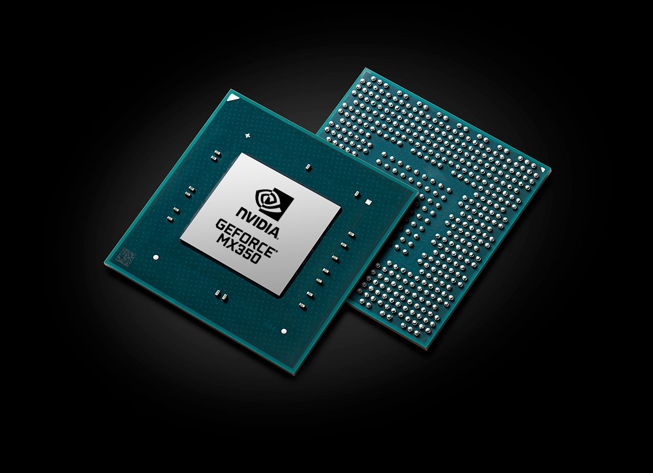
Nvidia has quietly launched the GeForce MX350 and MX330. The new mobile graphics cards are here to replace their respective MX200-series counterparts that debuted just one year ago. The new Turing-powered MX graphics cards should land in the second half of this year.
The GeForce MX350 is based on Nvidia's GP107 die from the Pascal days. This is the same silicon hidden inside the GTX 1050 and GTX 1050 Ti. In the MX350's case, it only comes with 640 CUDA cores though, whereas the the GTX 1050 has 640 (2GB) or 768 (3GB) and the 1050 Ti has 768.
The GeForce MX350 and GeForce GTX 1050 might have similar dies and can have the same CUDA core count, but there should be a sizable performance gap between them. The GeForce MX350 sports 32 TMUs (texture mapping units), 16 ROPs (render output units) and a 64-bit memory bus. However, the GeForce GTX 1050 flexes 40 TMUs, 32 ROPs and a 128-bit memory interface. Not to mention that the GTX 1050 has a 75W TDP, which gives it more breathing room.
As for its other specifications, the GeForce MX350 features a 1,354 MHz base clock and 1,468 MHz boost clock. The 2GB of GDDR5 memory runs at 7 Gbps across a 64-bit memory interface to output a memory bandwidth of 56.7 GBps.
Specs
| Header Cell - Column 0 | GeForce MX350 | GeForce MX250 | GeForce MX330 | GeForce MX230 |
|---|---|---|---|---|
| GPU Architecture | Pascal (GP107) | Pascal (GP108) | Pascal (GP108) | Pascal (GP108) |
| Shading Units | 640 | 384 | 384 | 256 |
| Texture Units | 32 | 24 | 24 | 16 |
| ROPs | 16 | 16 | 16 | 16 |
| Base Clock Rate | 1,354 MHz | 1,519 MHz | 1,531 MHz | 1,519 MHz |
| Boost Clock Rate | 1,468 MHz | 1,582 MHz | 1,594 MHz | 1,582 MHz |
| Memory Clock | 7 Gbps | 6 Gbps | 6 Gbps | 6 Gbps |
| Memory Capacity | 2GB GDDR5 | 2GB GDDR5 | 2GB GDDR5 | 2GB GDDR5 |
| Memory Bus | 64-bit | 64-bit | 64-bit | 64-bit |
| Memory Bandwidth | 56.06 GBps | 48.06 GBps | 48.06 GBps | 48.06 GBps |
| L2 Cache | 512KB | 512KB | 512KB | 512KB |
| TDP | 25W | 25W | 25W | 25W |
| Transistor Count | 3.3 billion | 1.8 billion | 1.8 billion | 1.8 billion |
| Die Size | 132 mm² | 74 mm² | 74 mm² | 74 mm² |
The GeForce MX330, on the other hand, continues to leverage the GP108 die. It has 384 CUDA cores with base and boost clock speeds up to 1,531 MHz and 1,594 MHz, respectively. In essence, the GeForce MX330 is a slightly overclocked GeForce MX250.
The graphics card also has 2GB of GDDR5 memory communicating across a 64-bit memory bus, just like the GeForce MX350. However, the memory here is clocked at 6 Gbps, so the memory bandwidth is down to 48.06 GBps.
Both the GeForce MX350 and MX330 target laptops, so they abide to strict TDP standards. The pair operate within the 25W restriction.
Get Tom's Hardware's best news and in-depth reviews, straight to your inbox.
GeForce MX350 and MX330 Benchmark Results
Although Nvidia just lifted the curtains off the GeForce MX350 and MX330, there are already early reviews of both SKUs. It's important to keep in mind that the MX-series is on the lower end of the spectrum. While the GeForce MX350 and MX330 are generally better than integrated graphics, they are nowhere near as powerful as Nvidia's GTX 16-series, and any gaming would have to be limited to low or very low settings at low resolutions.

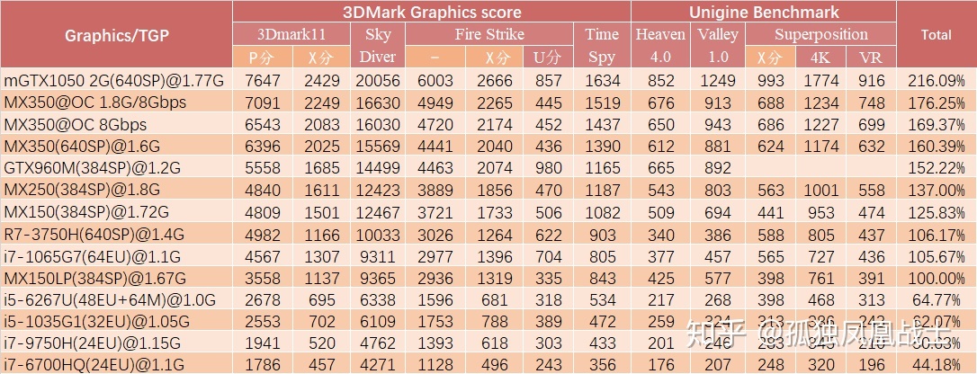
A user on Chinese website Zhihu ranked the GeForce MX350 between the GTX 1050 and GTX 960M in terms of performance. The GeForce MX350 reportedly held a healthy performance improvement over the GeForce MX250 but still fell far behind the GTX 1050. Notebookcheck's review lends credence to the validity of the results from the Zhihu review. Ultimately, it looks like we can look at the GeForce MX350 like a gimped GTX 1050 with a performance that's in the same ballpark as the GTX 960M.
Given the similar specifications, the GeForce MX330 should deliver the same level of performance as the GeForce MX250.
Pascal Rides Into the Sunset?
According to Notebookcheck's sources, the GeForce MX350 and MX330 could represent the mighty Pascal's last rodeo. Nvidia is reportedly working on a Turing-powered replacement for the GeForce MX350 to rival Intel's Xe DG1 mobile graphics solutions.
The Turing successor to the GeForce MX350 is internally known as N18S-G5. It allegedly taps into Nvidia's TU117 silicon, which the chipmaker uses in the GeForce GTX 1650. The TU117 die houses up to 1,024 CUDA cores, but the possibility of the N18S-G5 having all of them at its disposal is pretty slim.
The N18S-G5 is believed to feature PCIe 4.0 support and a 25W TDP. It seems that it will be available in two different flavors. The A variant is rumored to measure 23 x 23mm and the B variant at 29 x 29mm.
The N18S-G5-A should be the more flexible of the two as it's expected to arrive with GDDR5 memory at 3.5 GHz or GDDR6 memory at 5 GHz, compared to the N18S-G5-B's GDDR6 memory at 5 GHz. Independent of the variant, both reportedly adhere to the the typical 64-bit memory interface.

Zhiye Liu is a news editor, memory reviewer, and SSD tester at Tom’s Hardware. Although he loves everything that’s hardware, he has a soft spot for CPUs, GPUs, and RAM.