Researchers Create New CasFET Design for Next-Generation Transistors
Employing techniques learned from quantum physics to increase the lifetime of silicon-based transistors.

Researchers with Purdue University have reached a milestone in an attempt to design the next-generation transistor, which could allow for a life extension for silicon-based semiconductors. The new design, entitled CasFET (Cascade Field Effect Transistor) is yet another step on the road of transistor miniaturization, allowing for lower switching voltages, lower power consumption, and denser designs.
Tillman Kubis, the Katherine Ngai Pesic and Silvaco Research Assistant Professor of Electrical and Computer Engineering with Purdue, said this research comes in the face of increased difficulty in transistor miniaturization, which has seen increased technical difficulties and ballooning costs in recent years.
"They [transistors] need a high enough ON-current and low enough OFF-current, with a small enough difference to switch between both," Kubis said. "These challenges have significantly slowed the downscaling of transistors around the last eight years, making it increasingly difficult to introduce more powerful CPU generations." One of the more recognizable cases of this difficulty was Intel's transition to 10nm and 7nm processes, which saw a number of delays that have helped AMD's "unzenly" resurgence in the CPU space.
Article continues belowSamsung is employing GAAFET (Gate All Around Field Effect Transistor) technology for their 3nm process, with mass production expected for this year. The technology, a successor of FinFet, redesigns transistors to feature four gates on all four sides of a channel. This provides better transistor insulation from its neighbors, limits voltage leaks, and allows for lower voltages to be applied for the same switching effect. This in turn allows for more transistors to be deployed tighter together, increasing density. Samsung says this approach allows for a 35% size reduction in transistor design (compared to 5nm FinFET). However, it's expected that GAAFET will be exhausted sooner than FinFet ever was.

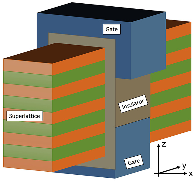
The development of CasFET comes as a next possible step in transistor manufacturing design, and deploys superlattice structures that are perpendicular to the transistor's transport direction, which allows for switchable cascade states. This actually employs effects learned from quantum cascade lasers, and essentially allows for more fine-grained voltage control. That's been one of the limiting factors in semiconductor scaling.
The team is currently developing the first CasFET prototype, and are still in the design stage for the overall structure and materials, trying to find the right balance between cost, material availability, ease of transition from typical transistor manufacturing, and performance. For now, the prototype doesn't offer the performance profile they're looking for. However, the work is promising enough that Purdue has applied for patent protection with the U.S. Patent and Trademark Office.
Get Tom's Hardware's best news and in-depth reviews, straight to your inbox.

Francisco Pires is a freelance news writer for Tom's Hardware with a soft side for quantum computing.