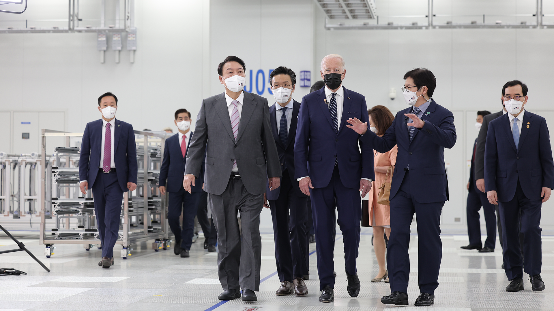
Samsung Showcases Advanced 3nm Chips to U.S., South Korean Presidents
Samsung demons 3GAE chip as it is gearing for high-volume production.

Samsung on Friday demonstrated the industry's first chip made using its 3 nm-class process technology featuring gate-all-around type transistors to Joe Biden and Yoon Suk-yeol, presidents of the U.S. and South Korea. The company is on track to start high-volume manufacturing of chips using its 3GAE technology in Q2 2022.
On Friday, Joe Biden arrived at the U.S. Osan Air Base in South Korea and immediately headed to Samsung's flagship semiconductor manufacturing facility near Pyeongtaek, which is currently the world's only fab that can produce chips using the company's 3 nm-class process technology. South Korean president Yoon Suk-yeol joined President Biden at the chip plant, reports The Korea Economic Daily.
There is no word which 3nm chip was shown to the U.S. leader and whether it was a live demonstration or a static showcase. Keeping in mind that Samsung Foundry is about to start HVM using its 3GAE node this quarter, it probably has working samples of its 3nm system-on-chip(s), though details of the demo are unknown.
"I have just seen how this plant makes the most advanced semiconductor chips in the world," said Biden. "They are a wonder of innovation and design, precision and manufacturing. "[…] When it comes to the most advanced chips, like the ones made here at Samsung — it is only one of only three companies in the world that makes these chips. It is an incredible — an incredible achievement."

One important aspect of the fab near Pyeongtaek is that it represents a great example of international collaboration in leading-edge semiconductor manufacturing. The fab uses extreme ultraviolet (EUV) lithography tools developed and built in the Netherlands that rely on light sources designed and made in the United States. The fab also heavily uses leading-edge equipment produced by U.S.-based companies Applied Materials, KLA, and LAM Research as well as many tools built in South Korea. Meanwhile, most electronic design automation tools used to design chips produced at gigafabs like the one near Pyeongtaek also originate from the United States.
"This plant also reflects the close bonds in innovation between our countries," said President Biden. "Much of the technology and machinery that is used to make these chips was designed and produced in the United States. By uniting our skills and our technological know-how, it allows the production of chips that are critical to both our countries and are essential sectors of our global economy."
Samsung claims that its 3GAE process will enable a 30% performance boost or a 50% power consumption reduction along with an up to 80% higher transistor density increase (including a mix of logic and SRAM transistors) compared to its 7LPP fabrication technology.
Get Tom's Hardware's best news and in-depth reviews, straight to your inbox.

Anton Shilov is a contributing writer at Tom’s Hardware. Over the past couple of decades, he has covered everything from CPUs and GPUs to supercomputers and from modern process technologies and latest fab tools to high-tech industry trends.
-
Alvar "Miles" Udell Considering how Samsung is falling back from their competitors in many segments, it needs to be otherworldly tech so they can catch up.Reply -
jp7189 I'm really excited by this. FinFET was a huge leap for transistors and this is an even bigger one IMO. There are so many parameters that can be tweaked in these gates to yield different transistor behavior. I wonder how flexible this 1st gen will be, and likewise how optimized the EDA tools are.Reply -
isofilm Samsung's wafer yield lies are so egregious, the South Korean Government is currently investigating them AGAIN. Samsung's Vice Chairman (Lee Jae Yong) was just released from prison for embezzlement and bribery and had to be given a special pardon to meet with Biden.Reply
Samsung 3nm yields are still in the 20% range, and anything Samsung claims to the contrary, are lies (forward looking statements), by their own admission. They have repeatedly and continuously lied about their 5nm, 4nm, and 3nm yields, and after recently getting caught lying, admitted they were lying to their wafer customers, now suddenly we are supposed to believe they have miraculously improved yields.
TSMC doesn’t start production until yields are around 70%, and shortly after production mature yields are around 90%.
The truth will be revealed soon enough, when both Samsung and Intel are forced to admit that their latest and most overly promised nodes are late, and then late again, and for the 3rd time late again, and .... -
watzupken Maybe they forgot to inform that the chip on demo is the only working chip that they are got out of the entire wafer. Getting a working chip out is difficult, but getting good yields is more important.Reply