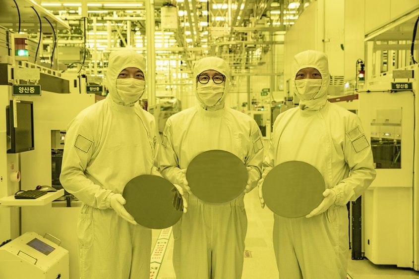
Samsung Will Produce 3nm Server CPUs for Unknown Company
Samsung lands another 3nm order, this time for a server processor.

Samsung Foundry has landed an order to make a server-grade processor using a 3nm-class process technology with gate-all-around (GAA) transistors for an overseas company, according to a press release by ADTechnology, a South Korean contract chip designer. The 2.5D system-in-package will use a 3nm chiplet or chiplets coupled with HBM memory.
"We are pleased to announce our 3nm design collaboration with AD Technology," said Jung Ki-Bong, Vice President of Samsung Electronics Foundry Business Development team. "This project will set a good precedent in the collaboration program between Samsung Electronics Foundry Division and our ecosystem partners, and Samsung Electronics Foundry Division will strengthen our cooperation with partners to provide the best quality to our customers."
Samsung has at least three 3nm-class process technologies featuring GAA transistors in its roadmap. The company currently uses its 'early' SF3E production node to make chips for cryptocurrency mining. Still, next year, the company will have an SF3 technology aimed at more advanced system-on-chips (SoCs) for various applications, including potentially server-grade products. In addition, the company has a performance-enhanced SF3P manufacturing process that better fits server processors.
Neither ADTechnology nor Samsung Foundry disclose what kind of SoC they are set to develop and produce for which company. Also, Pulsenews claims that the client is from the U.S. We only know that it is aimed at data centers, is made on a 3nm process technology, uses HBM memory, and is developed by a company that preferred to hire a contract chip designer to implement it. In theory, the processor could be one of many AI-oriented chips that are currently in development. Yet, this is a speculation on our part.
"This 3nm project will be one of the largest semiconductor products in the industry," said Park Joon-Gyu, chief executive of AD Technology. "This 3nm and 2.5D design experience will be a significant differentiation factor between other companies and AD Technology. We will do our utmost to deliver the best design results to our customers."
Get Tom's Hardware's best news and in-depth reviews, straight to your inbox.

Anton Shilov is a contributing writer at Tom’s Hardware. Over the past couple of decades, he has covered everything from CPUs and GPUs to supercomputers and from modern process technologies and latest fab tools to high-tech industry trends.
-
gg83 I wonder why crypto miners are willing to use the latest 3nm chip from Samsung. Do they get a better deal by using a less perfected node? Or is the benefit that much greater?Reply -
TryRebooting Reply
Smaller nodes use less power and crypto mining chips are ASICs (Application Specific Integrated Circuits) which means their design is far simpler as they are built to do 1 application efficiently.gg83 said:I wonder why crypto miners are willing to use the latest 3nm chip from Samsung. Do they get a better deal by using a less perfected node? Or is the benefit that much greater?
