DDR5/DDR4 Solution for 5nm SoCs Launched
Synopsys enables DDR4/DDR5 support on N5 designs.

Synopsys has started offering its DDR5/DDR4 physical interface (PHY) and controller for next-generation system-on-chips (SoCs) that will be made using TSMC's N5 (5 nm) fabrication technology. The IP package enable makers of SoCs to add support for both types of memory on their chips set to be made using TSMC's N5 node. Synopsys is the first IP company to offer a memory solution that supports both DDR4 and DDR5 with up to 6400 MT/s data transfer rates.
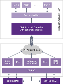
Synopsys' DesignWare IP package for DDR5/DDR4 memory implementations is rather advanced. It includes a DDR5/DDR4 controller that features a command scheduler, memory protocol handler, optional ECC memory, dual-channel support, and the DFI 5.0 interface to its PHY. The block supports 64 CAM entries for reads, 64 CAM entries for writes, and latencies as low as 8 clock cycles. The controller can be programmed using Arm's AMBA 3.0 APB interface. In addition, the company offers its silicon-proven DDR5/DDR4 physical layer (via Design & Reuse) that supports data transfer rates of up to 6400 MT/s as well as memory subsystems with up to four physical ranks. Obviously, both the controller and the PHY support all the JEDEC-standard capabilities of DDR4 and DDR5.
The IP package that Synopsys offers allows developers of various chips (CPUs, SoCs, SSD controllers, etc.) to throw the controller IP and physical interface into their N5 design and then verify that everything works correctly using the verification IP provided designed by the company.

https://www.tomshardware.com/reviews/what-is-fhd-full-hd,5741.html
Get Tom's Hardware's best news and in-depth reviews, straight to your inbox.

Anton Shilov is a contributing writer at Tom’s Hardware. Over the past couple of decades, he has covered everything from CPUs and GPUs to supercomputers and from modern process technologies and latest fab tools to high-tech industry trends.