TSMC Shows Colossal Interposer, Says Moore’s Law Still Alive
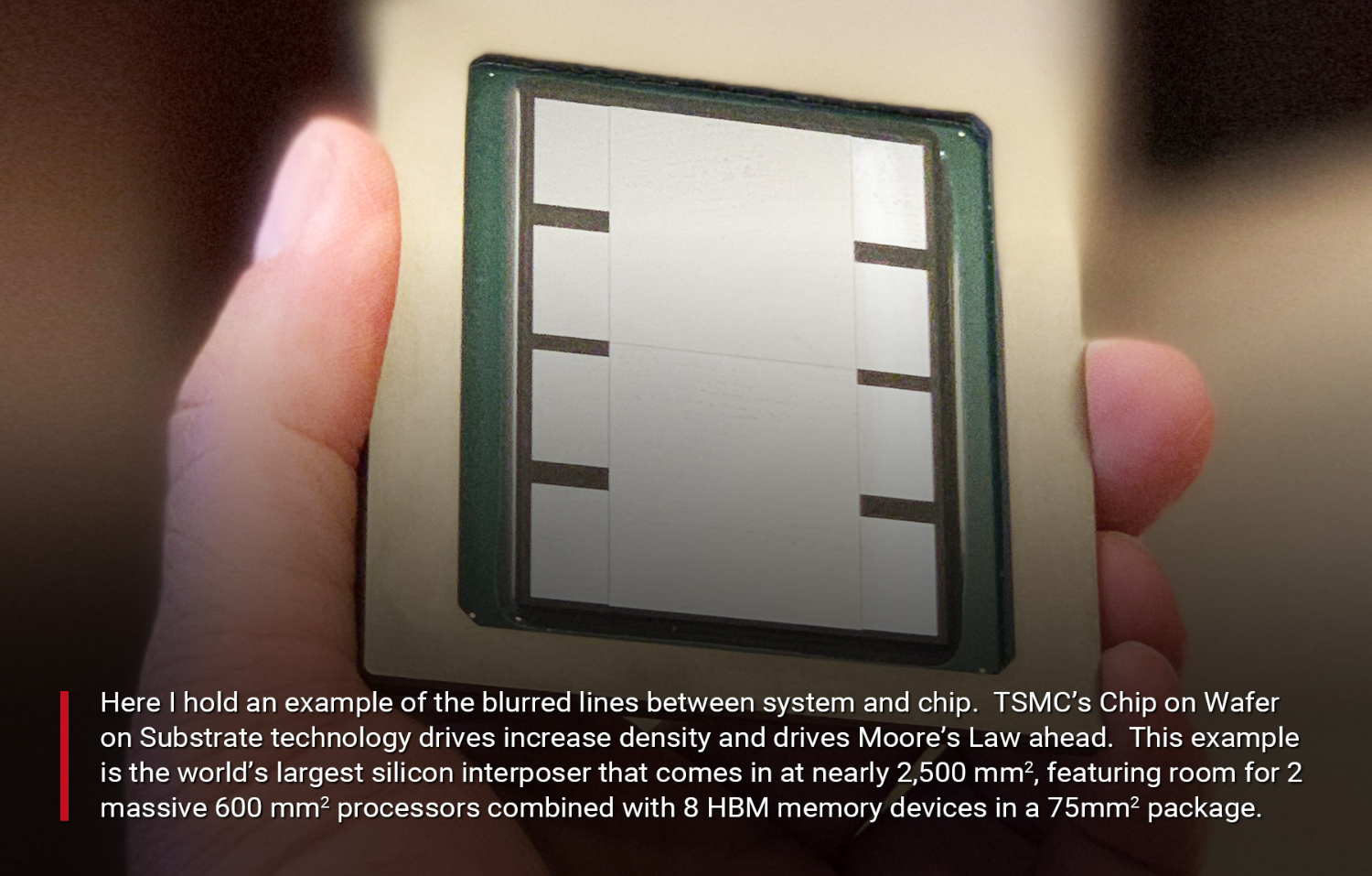
In the company’s first blog post, TSMC has stated that Moore’s Law is still alive and well, despite the zeitgeist of recent times being the reverse. The company also showed a colossal 2500mm2 interposer that includes eight HBM memory chips and two big processors.
Godfrey Cheng, TSMC’s new head of global marketing, wrote the blog post. He notes that Moore’s Law is not about performance, but about transistor density. While performance traditionally improved by increasing the clock speed and architecture, today it is more often improved by increasing parallelization, and hence requires increases in chip size. This enhances the importance of transistor density because chip cost is directly proportional to its area.
TSMC is addressing this with its latest N5P process node, an improved version of the company’s N5 node that TSMC announced a few weeks ago. The node will offer 7% higher performance or 15% lower power consumption compared to N5 and is expected in 2021. Cheng says it will have the world’s highest transistor density, although by that time Intel’s 7nm process might have taken that crown. But TSMC says 5nm is not the end.
Article continues below"After being exposed to our technology roadmap, I can safely state that TSMC has many years of pioneering and innovation ahead of us where we will continue to shrink the individual transistor and continue to improve density. You will hear more from us in the coming months and years as we progress to new nodes."
Scaling is of course constrained by atomic limits. Current transistors have a gate length of ~20nm, while a water molecule has a size of 0.275nm. One example that is given of a possible way to continue scaling are 2D materials, of which multiple layers could be stacked on a chip. As Cheng explains:
"By potentially using these new materials, one possible future of great density improvements is to allow the stacking of multiple layers of transistors in something we call Monolithic 3D Integrated Circuits. You could add a CPU on top of a GPU on top of an AI Edge engine with layers of memory in between. Moore's Law is not dead, there are many different paths to continue to increase density."
He then goes on to talk about system-level performance. It is important to keep chips such as CPUs, GPUs and AI processors fed with data, so it is critical to provide memory that is close to the cores for lower latency and energy. TSMC says we have transitioned from an era of design-technology co-optimization (DTCO) to system-technology co-optimization (STCO).
Get Tom's Hardware's best news and in-depth reviews, straight to your inbox.
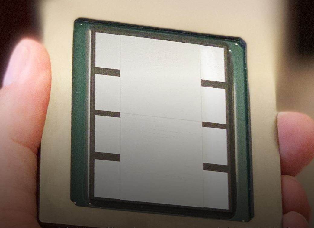
This is done through advanced packaging, for which TSMC supports silicon-based interposers and fan-out-based chiplet integration. It also has techniques to stack chips on wafers, or stack wafers on top of other wafers. As one such example, TSMC showed a nearly-2500mm2 silicon interposer – the world’s largest – on top of which two 600mm2 processors are placed and eight 75mm2 HBM memory chips, which makes for 1800mm2 of compute and memory silicon on top of the interposer-based package, well over two times the conventional reticle size limit.
TSMC is not the only company working on advanced packaging, as Intel recently showed some of its own impressive packaging feats.
In a separate bit of news, Digitimes reported on Wednesday that TSMC is investing $6.5 billion in a fab expansion to increase capacity. It also says that the company is slightly increasing its capital expenditures forecast for the year (to over $11 billion, while the previous estimate was $10-11 billion), indicating that demand is better than expected.
-
alextheblue Not dead yet, eh? I'm picturing a scene from Monty Python... and another one from Austin Powers.Reply -
redgarl So, by going with stacking, they are pretending that Moore's law is still going to be a thing...Reply
But in reality it is not. Density is density, it is not by adding a layer that you get more transistors per layer.

