A new PCB design can boost heat dissipation by 55x – copper coins placed under heat generating components drop temps drastically
Ideal for applications where cooling fans or heatsinks aren't practical.
OKI Circuit Technology has announced a new printed circuit board (PCB) design that can boost component heat dissipation by up to 55x. The Japanese firm has been developing and manufacturing PCBs for over 50 years and its portfolio stretches across a wide range of applications. This particular innovation, where a PCB is packed with stepped circular or rectangular copper coins, is headed to markets where even the best air coolers are impractical – like miniature devices or applications in outer space.
Heat dissipation is one of the problems that engineers involved with high-power electronics frequently have to overcome. One of the most common ways to address overheating components on a PCB is to add a heatsink, or even go active and install a fan. However, things like fans aren't always practical. In space, no one can hear your CPU scream, and it won't be cooled by a fan, as there is no air.
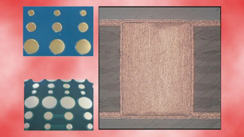
If you check out OKI's High Current / High Heat Radiation Board product pages you will see that it already had a PCB solution using embedded copper coins, thick copper foil wiring, and metal core wiring. Now it has finessed the copper coins by using stepped coin thicknesses and a choice of circular or rectangular coins – per your design preference.
Where OKI says coins, it is describing a copper structure that is rather like a rivet. Also, where it says stepped, it means that one end of the coin, or rivet, is a different size from the other. It gives the example of a stepped coin with a diameter of 7mm at the bonding surface with an electronic component, and 10mm at the heat-dissipating surface.
"The newly developed stepped copper coin features a larger heat-dissipating area relative to the bonding surface with the heat-generating electronic component to improve heat conduction efficiency," OKI explains. Then it goes on to say how its new rectangular coins are great for wicking the heat from traditionally rectangular heat-generating electronic components.
OKI's PR suggests this PCB technology might be best used in miniature and space applications – and it is in the latter case where it is said to boost heat dissipation by up to 55x. However, we immediately wondered if it could benefit PC components and systems,
Component makers like Asus, ASRock, Gigabyte, and MSI often boast about their lavish use of copper in motherboards and other components. Perhaps OKI's new stepped copper coins would be beneficial, too. These coins can extend through the PCB to conduct heat to large metal casings, suggests OKI. They could potentially connect to backplates and other cooling apparatus.
Stay On the Cutting Edge: Get the Tom's Hardware Newsletter
Get Tom's Hardware's best news and in-depth reviews, straight to your inbox.
Mark Tyson is a news editor at Tom's Hardware. He enjoys covering the full breadth of PC tech; from business and semiconductor design to products approaching the edge of reason.
-
The Historical Fidelity I think this stepped design is going to work well in exo-atmospheric conditions. Our endo-atmospheric electronics have the benefit of utilizing 2 separate heat transfer methods to release heat into the environment (radiation and convection) whereas exo-atmospheric only has one (radiation). So it makes sense that the stepped coin has a larger diameter at the other end of the chip being cooled in order to improve the heat dissipation if relying solely on the stepped coin for cooling, or efficiently using the stepped coin to act like a thermal vacuum to transfer heat to the next piece of the radiative cooling method (IE the larger side of the stepped coin can move more heat energy if each side is the same temperature (but lower than the heat source temperature), this creates a thermal gradient between the sides of the coin that then makes thermal transfer more effective through the coin using the thermal conductivity formula: watts per meter-kelvin where kelvin is the delta temperature between the sides of the coin).Reply
https://upload.wikimedia.org/wikipedia/commons/9/9a/Simple_definition_of_thermal_conductivity-en.svgRadiative heat dissipation requires a lot of surface area to transition thermal energy into infrared radiation that can be released into a vacuum efficiently in order to achieve a similar dissipation rate to endo-atmospheric equivalents. -
Findecanor I think I've seen similar solutions before. I don't know enough about the technology to understand what is novel about this one in particular.Reply
It is also commonplace on very conventional processes to have component footprints with large copper pads on both sides of a PCB and a dense grid of vias in-between them. -
Steve Nord_
I for one welcome our new discouragement of extraatmospheric copper theft using anodized or graphene fill slug PCBs. (Or is it Millions for launch and nothing for treaty, I forgot.)The Historical Fidelity said:I think this stepped design is going to work well in exo-atmospheric conditions. Our endo-atmospheric electronics have the benefit of utilizing 2 separate heat transfer methods to release heat into the environment (radiation and convection) whereas exo-atmospheric only has one (radiation). So it makes sense that the stepped coin has a larger diameter at the other end of the chip being cooled in order to improve the heat dissipation if relying solely on the stepped coin for cooling, or efficiently using the stepped coin to act like a thermal vacuum to transfer heat to the next piece of the radiative cooling method (IE the larger side of the stepped coin can move more heat energy if each side is the same temperature (but lower than the heat source temperature, this creates a thermal gradient between the sides of the coin that then makes thermal transfer more effective through the coin using the thermal conductivity formula: watts per meter-kelvin where kelvin is the delta temperature between the sides of the coin).
https://upload.wikimedia.org/wikipedia/commons/9/9a/Simple_definition_of_thermal_conductivity-en.svgRadiative heat dissipation requires a lot of surface area to transition thermal energy into infrared radiation that can be released into a vacuum efficiently in order to achieve a similar dissipation rate to endo-atmospheric equivalents. -
frankens Placing copper under hot components has been a pretty standard practice for 50 years. Some components are even soldered to this large copper 'coin'. Standard for most non heat sinked power transistors/ drive circuits. Also introduces a ground plane to reduce noise. Pretty common in the radio industryReply -
The Historical Fidelity
Not integrated into a PCB, so not really relevant in my opinionfrankens said:Placing copper under hot components has been a pretty standard practice for 50 years. Some components are even soldered to this large copper 'coin'. Standard for most non heat sinked power transistors/ drive circuits. Also introduces a ground plane to reduce noise. Pretty common in the radio industry -
bit_user This reminds me of a backside-cooling experiment I tried with a SoC, earlier this year:Reply
https://forums.tomshardware.com/threads/how-much-does-cooling-the-underside-of-the-motherboard-cpu-typically-help.3844807/post-23269204 -
The Historical Fidelity
Very cool! And nice write-up!bit_user said:This reminds me of a backside-cooling experiment I tried with a SoC, earlier this year:
https://forums.tomshardware.com/threads/how-much-does-cooling-the-underside-of-the-motherboard-cpu-typically-help.3844807/post-23269204 -
kjfatl
I'm having difficulty understanding what is 'new' here that we have not been doing for decades. An close array of vias, plated solid with copper under the 'exposed pad' of part above. What are they doing different? Cutting a hole in the PCB and filling it with a copper slug? If so, they might double the thermal capacity over standard design practice. For this to be optimal, the slug would have to be inserted before plating the through-hole vias in order to insure good thermal connections to inner layer planes. I wish this had been better explained in the article. Nothing stands out on the supplier's website either.The Historical Fidelity said:Not integrated into a PCB, so not really relevant in my opinion -
Conor Stewart What is new here? This is just a heatsink in a different form factor. Normally heat sinks are placed on top of a component, these are just placed under them. Like has already been mentioned thermal pads already exist for this purpose, yes these might be better but for most uses they probably aren't that much better.Reply
Radiative cooling depends on surface area and your limiting factor in cooling will likely be how much you can radiate, not conducting the heat to the radiative surface, so an exposed copper pour on the PCB connected to the thermal pad under the component with vias would likely be as good in a lot of circumstances. -
Johnpombrio Reminds me of seeing a PCB used for military aircraft. It had a large sheet of metal over the board to create a Faraday cage around the card to prevent EMP damage. Trying to probe the board to see if it worked properly was a nightmare.Reply