Intel completes assembly of first commercial High-NA EUV chipmaking tool — addresses cost concerns, preps for 14A process development in 2025
Transistor shrinking intensifies.

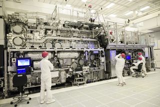
Intel Foundry announced Thursday that it had completed the assembly of the industry's first commercial High Numerical Aperture (High-NA) Extreme Ultraviolet (EUV) machine in its D1X fab in Oregon -- an important milestone as the company readies research and development for its 14A process in 2025.
Intel Foundry is the lead customer for toolmaker ASML's Twinscan EXE:5000 machine, beating commercial rival TSMC and others to begin R&D with the machine. Tom's Hardware spoke with Intel's Director of Lithography Hardware and Solutions to learn more about the new technology, and cost concerns that surround it.
The High-NA lithography tool will enable Intel to print features up to 1.7X smaller than possible with existing EUV tools, eventually allowing Intel to shrink to smaller transistors than possible with standard, Low-NA EUV machines, thus yielding up to a 2.9X transistor density improvement for a single exposure. In fact, ASML announced yesterday that the only other assembled High-NA machine, its pathfinding machine located in Veldhoven, Netherlands, had set a record for an EUV system by printing the first 10nm dense lines with a full-field lithography system.
Intel famously spent decades helping the industry develop first-gen Low-NA lithography technology, but chose not to use it for its 10nm process due to cost concerns. Instead, Intel chose to use quad-patterning with standard deep ultraviolet (DUV) lithography machines, requiring four DUV exposures for a single chip layer instead of a single exposure with EUV. As a result, Intel encountered numerous difficulties with yields, leading to five years of delays for its 10nm process.
As such, Intel remained mired on the 14nm node while long-time rival TSMC adopted EUV and took the lead in process node tech from Intel for the first time. TSMC then armed Intel's rivals, like AMD, with its better process tech, leading to significant market share losses for the product side of Intel's business.

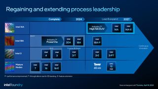
Intel finally adopted EUV technology with its 'Intel 4' process node, but the years of delays left it lagging several nodes behind TSMC. Intel says it is now on a course to retake the lead by launching five nodes in four years (5N4Y), an audacious initiative that remains on track for completion by the end of the year.
However, the job is never done and Intel is keen to make sure it adopts the latest technology to avoid the mistakes of the past. Intel is now looking to develop its newly announced 'Intel 14A' (1.4nm-class) process node and the follow-on 10A node (1nm) with High-NA EUV. Intel will first de-risk the tech by developing product proof points with its 18A node in 2025 and then begin developing its 14A node. Intel also plans to be an early adopter of ASML's second-gen Twinscan EXE:5200B system, which produces more than 200 wafers per hour (WPH), a marked improvement over the current-gen High-NA machine's 185 WPH throughput. Both of those machines are faster than ASML's flagship Low-NA EUV machine, which offers up to 160 WPH. Intel also says that ASML has three generations of its High-NA machines already in development.
Stay on the Cutting Edge
Join the experts who read Tom's Hardware for the inside track on enthusiast PC tech news — and have for over 25 years. We'll send breaking news and in-depth reviews of CPUs, GPUs, AI, maker hardware and more straight to your inbox.
Intel says it sees a runway to use High-NA for at least three process nodes, and perhaps more, so this technology will become a foundational component of its chipmaking operations for an extended period of time. Let's take a closer look at the tool.
ASML Twinscan EXE:5000 High-NA EUV Machine


The original introduction of EUV faced numerous delays, and the first-generation tools weren't production-ready when they first launched. In fact, the first shipping Low-NA tools required upgrades and took multiple years to be suitable for production.
EUV technology has matured, and ASML's approach to building the new High-NA Twinscan EXE:5000 is significantly more optimized. ASML's existing Low-NA Twinscan NXE:3600 EUV machines were used as a building block for the new High-NA machine. ASML's Low-NA models employ a modular design, allowing the company to leverage proven technology and modules for its new machine while improving other modules, thus speeding the development of the new machine. This modularity also allows the machines to be upgraded with newer, improved modules in the field.
ASML has also built test stands that allow each module to be tested individually, thus ensuring that each module delivers the basic functionality before the system is fully assembled. ASML builds many of the critical modules in the US. For instance, the light source module is built in San Diego, California, and the top module is built in Wilton, Connecticut.
In the past, ASML sent the completed modules for its development systems to its Veldhoven, Netherlands facilities, assembled the machine, ensured its functionality, dissembled the machine, and then shipped it to its partner. Naturally, shipping the modules back and forth across continents slowed the deployment process.
In contrast, ASML employed a parallel field integration strategy for Intel's High-NA machine that involved sending the pre-tested modules directly to Intel's Oregon fab. ASML shipped the modules to Intel via 350 crates placed inside 43 freight containers, which were then flown to Seattle in multiple cargo planes. Intel then used 20 trucks to bring the more than 150 metric tons of equipment to its Oregon fab. Intel CEO Pat Gelsinger recently said the machine cost '400-ish million' dollars.

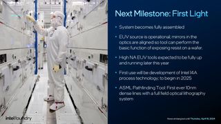
The process of installing and calibrating the machine will span six months. Intel has already reached the critical milestone of assembling the machine, with the next major milestone being the 'First Light.' This checkpoint involves conducting the basic function of exposing the resist on the wafer and signifies that the light source, mirrors, and optics are all functioning properly and aligned. ASML achieved First Light with its High-NA machine in February, and Intel will soon follow.


To speed the development of the High-NA tool, ASML preserved much of the existing foundation of its NXE machines. The High-NA tool employs the same 13.5nm EUV light wavelength, so the proven light source module required a new interface to support a minimal change to the source's angle that optimizes the optical transmission through the illuminator to maximize efficiency. However, the new system has a halved exposure field compared to Low-NA machines, meaning printing a single wafer could take twice as long. To solve this problem, ASML employed an optimized wafer stage for the NXE:5000 and it now accelerates at 8g — twice as fast as the prior generation. ASML also improved the reticle stage for a 4X speed improvement over the prior generation — this stage now accelerates roughly the same as a car going from zero to 60 MPH in 0.09 seconds.
The smaller exposure field still halves the maximum size of a single die that can be created with a single exposure. Intel says it is working with its EDA partners (many of which joined the company on stage at its IFS Direct event) to integrate stitching tools into the software used for chip design, thus allowing stitching together two separately exposed regions of the wafer to create a single larger die. This effort will take time to come to fruition because it has to be addressed during the design phases of a processor, but optimized EDA software will enable printing larger die sizes for Intel and its customers. It will also allow Intel to better utilize its other full-field tools.
Much of the existing technology, such as basic mask technology, multi-layer optics coatings, and basic resist technology, also carries over to the new machine.
The biggest challenge was developing new optics. Reducing the tools' critical dimension (CD—the smallest feature that can be printed) typically requires either reducing the wavelength of the light source or adjusting the numerical aperture (NA—a measure of the ability to collect and focus light). A higher NA delivers higher imaging contrast and enables using less light per exposure, speeding production. ASML employs the same 13.3nm light wavelength for its High-NA machine as it does with Low-NA, so the biggest advance was moving from 0.33 NA with Low-NA tools to 0.55 NA with the High-NA tool.
ASML and Zeiss worked together to develop the new anamorphic optics and improved the printing resolution by using bigger mirrors and reducing the angle of the light hitting the reticle. These adjustments reduced the CD from 13nm with Low-NA to 8nm with High-NA. This advance enables printing the smallest features for sub-3nm process nodes with a single exposure.
Intel will initially use the High-NA machine largely for research and development, but will eventually use it for production. Intel says it is designing its 14A process from the ground up to unlock the benefits of High-NA in an unspecified number of critical layers of the design.
ASML has revealed that it has orders for 10 to 20 High-NA EUV machines and announced yesterday that it has begun shipping a second machine to an undisclosed customer.
Addressing High-NA Cost Concerns

The arrival of High-NA has been met with industry reports that it will be more expensive to use High-NA than multi-patterning with existing Low-NA EUV machines. Low-NA systems cost in the neighborhood of $185 million, whereas the new High-NA machine is said to be around $400 million, so cost has been thrust into the limelight. I asked Mark Phillips, Intel Fellow and Director of Lithography Hardware and Solutions, if the company sees this as the most cost-effective path forward.
Modern semiconductors are comprised of multiple layers, with each layer featuring various levels of complexity and different feature sizes. Phillips told us that Intel only plans to use High-NA for an unspecified number of critical layers that require the smallest feature sizes. In contrast, Intel will use older Low-NA EUV, 192nm ArFI, and even 248nm KrF DUV patterning for other layers, with the latter being employed for the upper interconnect layers with larger feature sizes. Intel is designing its 14A node from the ground up to leverage the superior single-exposure High-NA resolution in a few of the tightest-pitch critical layers. Phillips contends that High-NA is more cost-effective for these layers than multi-patterning.
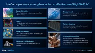
Intel will also employ Applied Materials' Centura Sculpta pattern shaping tool to improve its patterning capabilities and reduce costs. As you can see in this video, this directional etching technology 'pushes' features (Phillips notes this is preferable only in a single direction) to complement and improve the single-patterning capabilities of EUV lithography.
"And I would just add, it's not like ASML built this tool and then came to us and asked us if we want to buy it. We started working with ASML more than a decade ago, having these discussions about the business case for the tool," Phillips said. "What are the right tradeoffs of the tool cost versus the capability in order to make it a viable tool? So we knew those capabilities, those specs, and we knew the price when we committed to these tools years ago. And really, there haven't been surprises," said Phillips. He also said the tools perform to the agreements Intel made with ASML long in advance.
Phillips also noted that the High-NA tool would be useful in maximizing the impact of Intel's other new technologies, like its PowerVia Backside Power Delivery. "Backside power delivery, by being able to strip out all the metal lines on the front side stack that carry power and moving them to the backside, then we're able to re-optimize the metal stack on the front side of the wafer," Phillips said.
"It turns out that puts a number of layers right in the sweet spot for the use of the high end tool. So, if you use it for the things that it was designed to do, and you've had enough confidence that it was going to stay on schedule to plan your process to take advantage of them, then yes, it certainly is cost-effective." Phillips also sees High-NA as critical to developing interconnects for the vertically-stacked CFET transistors that will usher in the next wave of density increases (Intel hasn't put that revolutionary tech on its formal roadmap yet).
Intel also has extensive experience with its Directed Self-Assembly (DSA) technology, which uses special materials that can naturally self-assemble molecules into small and regular patterns on a wafer. This technology allows Intel to print with lower EUV light doses and then repair defects, like line edge roughness, thus boosting the speed of the patterning process while improving yields and lowering costs. Phillips says DSA isn't required to make High-NA economically viable. Intel also has several other complementary internal capabilities in its tool chest, such as its mask shop, which built the first EUV masks.
Intel plans to hit the ground running. ASML's High-NA machine in Veldhoven will come online first, and Intel plans to start working on its long lead time items, like its Optical Proximity Correction (OPC) models, on that machine as it waits for the full bring-up of its machine in Oregon.
Intel's next step in the process of deploying High-NA will be reaching the First Light milestone. The company hasn't set a date for that checkpoint yet, but it is obviously close to that goal. The tool will be used for the development of the 'Intel 14A' process in 2025.

Paul Alcorn is the Managing Editor: News and Emerging Tech for Tom's Hardware US. He also writes news and reviews on CPUs, storage, and enterprise hardware.
-
JayNor "TSMC then armed Intel's rivals, like AMD, with its better process tech, leading to significant market share losses for the product side of Intel's business."Reply
So Intel's introduction of Sierra Forest and Granite Rapids chips on Intel-3 should be expected to regain its process tech lead and recover significant market share over AMD? -
Giroro Intel 14A is not 1.4nm The name has nothing to do with the size. They were very clear on that when they when they tried (and succeeded) to get away with their misleading rebrand of 10 nm to Intel 7.Reply
They never gave us a roadmap of what process got renamed to 14A, but it's likely 2 or 3 nm. Granted transistor size has always been a big marketing trick; when they named their transistors in "nm", it still had little to no relation to physical size of any feature on any chip. But the point is 14A is almost certainly not going to outperform whatever tech TSMC is calling 2nm. -
peachpuff ReplyIntel says it is now on a course to retake the lead by launching five nodes in four years
-
thestryker After seeing how much bigger the High-NA machines are I couldn't help but wonder if that was going to impact adoption for some fabs. Intel mentioned that these cannot just be swapped in where EUV machines were unless the fab was already designed for it. It will be interesting to see how quickly ASML can ramp up production since the current rate is fairly low.Reply
A couple of article mistakes:
Intel finally adopted EUV technology with its 'Intel 7' process node, but the years of delays left it lagging several nodes behind TSMC.
Intel 4 not Intel 7
TSMC achieved First Light with its High-NA machine in February, and Intel will soon follow.
ASML not TSMC
Nothing since the shift to FinFET has been an accurate representation of size. Intel shifted the name of "10nm" because their competition is even less honest about node sizes and Intel's process is largely equivalent to TSMC N7.Giroro said:Intel 14A is not 1.4nm The name has nothing to do with the size. They were very clear on that when they when they tried (and succeeded) to get away with their misleading rebrand of 10 nm to Intel 7.
According to Intel's slides from their foundry presentation (Ian Cutress has them in his writeup) Intel 3 is still behind on process technology in more areas than not. 18A is when they should be hitting at worst equivalent in every area. They should be offering equivalent (or maybe even better as we haven't seen performance numbers) compute density with SRF/GNR though.JayNor said:So Intel's introduction of Sierra Forest and Granite Rapids chips on Intel-3 should be expected to regain its process tech lead and recover significant market share over AMD? -
Batweasel The jumpsuits and little red hats make this look like if SuperHot did a 70s James Bond supervillain lair level.Reply -
craigss Research ?Reply
On course?
Well they "researched " 10nm for many years whilst fools kept throwing money at them +++++++ many times, tbh they are doing it again aka 12xxxx to 14xxx there is no real change yet its claimed to be a new gen chip on 14....but we all know the truth
Most Popular


